SWCS059I March 2011 – November 2014 TPS80032
PRODUCT PREVIEW Information. Product in design phase of development. Subject to change or discontinuance without notice.
- 1Device Overview
- 2Revision History
- 3Terminal Configuration and Functions
-
4Specifications
- 4.1 Absolute Maximum Ratings
- 4.2 Handling Ratings
- 4.3 Recommended Operating Conditions
- 4.4 Thermal Characteristics for YFF Package
- 4.5
Electrical Characteristics
- 4.5.1 Switched-Mode Regulators
- 4.5.2 LDO Regulators
- 4.5.3 Reference Generator
- 4.5.4 Crystal Oscillator
- 4.5.5 RC Oscillators
- 4.5.6 CLK32KAUDIO Buffer
- 4.5.7 Backup Battery Charger
- 4.5.8 Switched-Mode System Supply Regulator
- 4.5.9 Battery Charger
- 4.5.10 Indicator LED Driver
- 4.5.11 USB OTG
- 4.5.12 Gas Gauge
- 4.5.13 GPADC
- 4.5.14 Thermal Monitoring
- 4.5.15 System Control Thresholds
- 4.5.16 Current Consumption
- 4.5.17 Digital Input Signal Electrical Parameters
- 4.5.18 Digital Output Signal Electrical Parameters
- 4.5.19 Digital Output Signal Timing Characteristics
- 4.6 Typical Characteristics
-
5Detailed Description
- 5.1 Real-Time Clock
- 5.2 Clocks
- 5.3 Power Management
- 5.4 Reset System
- 5.5 System Control
- 5.6 System Voltage/Battery Comparator Thresholds
- 5.7 Power Resources
- 5.8 Backup Battery Charger
- 5.9
Battery Charging
- 5.9.1 Charger and System Supply Regulator Controller Operation
- 5.9.2 System Supply Regulator
- 5.9.3 Battery Charging
- 5.9.4 Anticollapse Loop and Supplement Mode
- 5.9.5 Battery Temperature Monitoring
- 5.9.6 Safety Timer and Charging Watchdog
- 5.9.7 Limit Registers
- 5.9.8 Battery Presence Detector
- 5.9.9 Indicator LED Driver
- 5.9.10 Supported Charging Sources
- 5.9.11 USB Suspend
- 5.9.12 Support for External Charging IC
- 5.9.13 Battery Charger Interrupts
- 5.10 USB OTG
- 5.11 Gas Gauge
- 5.12 General-Purpose ADC
- 5.13 Vibrator Driver and PWM Signals
- 5.14 Detection Features
- 5.15 Thermal Monitoring
- 5.16 I2C Interface
- 5.17 Secure Registers
- 5.18 Access Protocol
- 5.19 Interrupts
- 6Recommended External Components
- 7Device and Documentation Support
- 8Mechanical Packaging and Orderable Information
Package Options
Mechanical Data (Package|Pins)
- YFF|155
Thermal pad, mechanical data (Package|Pins)
Orderable Information
5 Detailed Description
5.1 Real-Time Clock
The RTC is driven by the 32-kHz oscillator and provides the alarm and timekeeping functions. The RTC is supplied by the backup battery (when available) if the main battery fails and if no external power is applied.
The main functions of the RTC block are:
- Time information (seconds/minutes/hours) in binary coded decimal (BCD) code.
- Calendar information (day/month/year/day of the week) in BCD code up to year 2099.
- Programmable interrupts generation. The RTC can generate two interrupts:
- Timer interrupts periodically (1s/1m/1h/1d period) in the ACTIVE and SLEEP states (can be masked during the SLEEP period with the IT_SLEEP_MASK_EN bit in the RTC_INTERRUPTS_REG register in order to prevent the host processor from waking up)
- Alarm interrupt at a precise time of the day (alarm function) in the ACTIVE and SLEEP states and switch-on transition from the WAIT_ON state
- Oscillator frequency calibration and time correction with 1/32768 resolution.
For security purposes, the registers related to time and calendar information are protected by restricting their write access to software running in the secure mode of the host (the MSECURE pin set to 1). Read access is always allowed, even in a nonsecured mode. However, it is possible to disable the secure mode with the MSECURE OTP bit. In this case, the read and write accesses are available regardless of the status of the MSECURE pin.
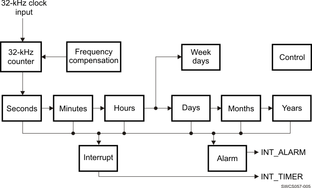 Figure 5-1 Block Diagram of the RTC Digital Section
5.2 Clocks
The TPS80032 device is independent of any high-frequency system clock; it provides only a 32-kHz clock to the platform. The oscillator can use an external crystal unit to generate the clock or use an external 32-kHz oscillator, in which case the internal oscillator module is bypassed.
To provide a high-performance 32-kHz clock for peripherals, like an audio device, a dedicated output buffer is implemented on the CLK32KAUDIO ball. This audio buffer uses the 1.8-V VRTC regulator as power. CLK32KAO is always active when 1.8-V I/O voltage is available, whereas the CLK32KG and CLK32KAUDIO outputs can be controlled by PREQ signals and register bits (CLK32KG_CFG_TRANS, CLK32KG_CFG_STATE, CLK32KAUDIO_CFG_TRANS, and CLK32KAUDIO_CFG_STATE).
The TPS80032 device also includes a 32-kHz RC oscillator and a 6-MHz RC oscillator, which are used internally.
5.3 Power Management
The power-management state machine manages control of the state of the different resources included in the TPS80032 device depending on system activity and energy availability. It ensures the detection of external or internal triggering events that initiate a change of system power state. It controls the transition sequences required to change the system from current power state to a new power state by configuring the resources according to the desired final power state.
Host processor can access the configuration registers using the general-purpose I2C interface (CTL-I2C). Figure 5-2 shows a block diagram of the power-management system.
 Figure 5-2 Block Diagram of the Power Controller
5.3.1 Finite State Machine (FSM)
The TPS80032 FSM controls boot sequences, TPS80032 state changes and resources initialization. The power sequences are stored in a hard coded table (OTP memory). The FSM reacts on events, which initiates power state transitions.
5.3.2 Hardware Events
- Starting events (going into ACTIVE state):
- Power on button (PWRON ball)
- Remote power on (Accessories) (RPWRON ball)
- Battery plug (VSYS ball)
- VAC detection (VAC ball)
- USB VBUS detection (VBUS ball)
- USB ID detection (USB ID ball)
- RTC alarm
- Stopping events (going into OFF state):
- Short PWRON key press (interrupt to the processor that initiates switch off)
- Long PWRON key press (hardware switch off)
- Remote power on (RPWRON) (interrupt to processor that initiates switch off)
- Primary watchdog expire (hardware switch off)
- Regulator short circuit protection (hardware switch off)
- Thermal shutdown (hardware switch off)
- Backup events or shutdown events (going into NO SUPPLY or BACKUP state):
- Removal of main and/or backup battery
- Low main and/or backup battery
5.3.3 Software Events
- Stopping events (going into OFF state):
- DEVOFF instruction: DEV_OFF register bit all set to one (PHOENIX_DEV_ON register)
- Software reset (SW_RESET), going to OFF state and then restart to ACTIVE
5.3.4 Resource Definition
A resource is an element that provides the necessary to a system to operate. Typical resources are supplies, clocks, resets, references, bias. Each resource can be addressed with its unique I2C address RES_ID (Resource Identification).
A remapping of the resource state versus the system state can be done. For example, a resource can be set either ON or OFF when the system state is SLEEP.
5.3.5 Resource Operating Modes
5.3.5.1 Voltage Regulator Operating Modes (All Types)
In order to optimize the power consumption, three operating modes may be allowed for a voltage regulator:
- OFF mode: The output voltage is not maintained and the power consumption is minimized.
- AMS mode: The regulator is able to deliver its nominal output voltage with a full load current capability. Quiescent current adapts automatically to load current.
- FORCE mode: Force active mode.
5.3.5.2 REGEN1 / REGEN2 / SYSEN Operating Modes
- DISABLE: The REGEN1 / REGEN2 / SYSEN I/O drives the signal to its disable state.
- ACTIVE: The REGEN1 / REGEN2 / SYSEN I/O drives the signal to its active state.
5.3.5.3 SMPS Operating Modes
- OFF mode: The output voltage is not maintained and the power consumption is minimized.
- AUTO mode: The SMPS is able to deliver its nominal output voltage with a full load current capability. PFM or PWM is automatically selected versus load current.
- FORCED_PWM mode: The SMPS runs always in PWM even at light load. It allows to maintain a low output voltage ripple.
5.3.5.4 Main Bandgap Operating Modes
- OFF mode: The reference voltage is not maintained and the bandgap power consumption is minimized.
- ON ACCURATE mode: The bandgap is able to deliver accurate nominal reference voltage.
- LOW POWER mode: A nominal but less accurate voltage reference is maintained with very low power consumption.
- ON FAST mode: The nominal reference voltage is maintained with less precision as the low pass filter on the VBG output is disabled. This condition during power up phase allows a quicker setting of the reference voltage. This mode is only used during a BOOT or WAKEUP phase.
5.3.5.5 Comparators Operating Modes
- OFF mode: The comparator is disabled, result of compare operation is forced to true, power consumption is minimized.
- ON mode: The comparator is enabled result of compare depends on its inputs.
5.3.5.6 Hot-die Warning Operating Modes
- ACTIVE mode: The hot-die warning feature is enabled.
- OFF mode: The hot-die warning feature is disabled.
5.3.5.7 Clocks and PWM1 / PWM2 Drivers Operating Modes
- DISABLE mode: The signal at driver output is stopped.
- ACTIVE mode: The signal at driver output is running.
5.3.6 Addressing Resources Registers
Three types of register can be associated to a resource:
- Configuration Registers:
- CFG_TRANS register
- CFG_STEP register (DVS resource)
- State Register:
- CFG_STATE register
- DVS Registers:
- CFG_FORCE register
- CFG_VOLTAGE register (DVS resource)
The configuration registers are intended for resource configuration, while state registers are intended to manage the resource state transition; finally DVS registers are intended to dynamic voltage control via DVS-I2C. Configuration and state registers contribute to determine resource behavior. The state register defines to which state the resource has to switch and the timing for the transition. The configuration register defines the resource behavior in a defined state. Although both types of registers can be access by the FSM and the CTL-I2C, it is preferable to reserve I2C access to configuration registers and FSM access to state registers. Access to DVS registers is exclusively done via DVS-I2C in applications using DVS capability.
These registers can be accessed in different ways, individual access to allow accessing registers through their physical address (ID) and broadcast messages that are interpreted by individual resources in function of their configuration
5.3.6.1 State Register (CFG_STATE)
Purpose of this register is to set the state of the resource. If the resource is associated to a Power request pin (PREQ1, PREQ2 or PREQ3), any state change of the Power request pin will be transmitted to all its associated resources.
5.3.6.2 State Mapping Register (CFG_TRANS)
Purpose of this register is to map the individual resource state to the state resulting from system states arbitration (RES_STATE).
5.3.6.3 Voltage Register (CFG_VOLTAGE)
This register is dedicated to resources belonging to the power provider category (LDO or SMPS), is used to set the voltage level of the SMPS and LDO.
5.3.6.4 Force Register (CFG_FORCE)
This register is dedicated to DVS-SMPS. It can be accessed through DVS-I2C and power management control FSM during power on sequence. This is used to force the voltage without ramping.
5.3.6.5 Step Register (CFG_STEP)
This register is dedicated to DVS-SMPS; its purpose is to control the slope of voltage ramping when VSEL content is modified.
5.3.7 Power Management I/Os Functionality
5.3.7.1 BOOT[2:0]
Purpose of these input balls is to select the boot sequence executed by the TPS80032 device during the startup phase. BOOT [2:0] balls provide indication on the following parameters to select the correct value for the supply voltages and detection thresholds (see PH_STS_BOOT register).
- BOOT0: Battery chemistry (cut-off voltage), described in EPROM Application Note.
- BOOT1: Described in EPROM Application Note.
- BOOT2: Described in EPROM Application Note.
5.3.7.2 PWRON
The PWRON ball is intended to be connected to a push button to control system power on / off. An internal pull up on the battery domain is implemented on this input.
Three timers are associated to this input duration:
- A short timer of 15ms to confirm the key press detection; this confirmation initiates a power-on sequence or generation of an interrupt depending on system state.
- A long timer, programmable from 50 ms to 1.55 seconds, that measures the key press. A register bit (KPD_STS bit in KEY_PRESS_DURATION_CFG register) is set and an interrupt (SPDURATION) is generated if the key press duration exceeds the timer duration.
- A very long timer of 8 or 4 seconds (the duration is selected with LPK_TIME bit in KEY_PRESS_DURATION_CFG register) that generates a shutdown by forcing the TPS80032 device to the WAIT-ON state. The shutdown reason is indicated by a register bit (DEVOFF_LPK in PHOENIX_LAST_TURNOFF_STS register). The shutdown feature can be disabled by an OTP memory bit (LPK_DISABLE) and there is another OTP memory bit (LPK_RESTART) which can be used to generate a startup just after the transition to WAIT-ON.
PWRON detection is performed on both falling and rising edges (1 interrupt line, 1 interrupt status bit). The polarity is defined as following:
- High level: Key released
- Low level: Key pressed
5.3.7.3 RPWRON
RPWRON is also intended to control the system power on / off. An internal pull up on the battery domain is implemented on this input. One timer is associated to this input duration:
- A short timer of 15ms to confirm detection, this confirmation initiates a power-on sequence or generation of an interrupt depending on system state.
RPWRON can be programmed with OTP bit (RPWRON_OFF_DIS) to generate a shutdown sequence. In this situation there is 1 second delay between the interrupt generation and the shutdown sequence.
RPWRON detection is performed on both falling and rising edges. The polarity is defined as following:
- High level: Key released
- Low level: Key pressed
5.3.7.4 REGEN1, REGEN2
The power management FSM controls these output signals. These balls are activated during the power on / power off sequences. The timing of activation is dependant of the power sequence (OTP memory). REGEN1 and REGEN2 can be used to control two different external power supplies. The associated registers are:
- REGEN1_CFG_TRANS, REGEN1_CFG_STATE
- REGEN2_CFG_TRANS, REGEN2_CFG_STATE
The polarity is defined as following:
- High level: Active
- Low level: Disabled
5.3.7.5 SYSEN
This output signal is controlled by the power management FSM, is activated during the power on / power off sequences. The timing of activation is dependant of power sequence. SYSEN can be used to control an external power supply or a slave PM device. SYSEN related registers are:
- SYSEN_CFG_TRANS, SYSEN_CFG_STATE
The polarity is defined as following:
- High level: Active
- Low level: Disabled
5.3.8 PREQ1, PREQ2, PREQ3 Hardware Commands
ACTIVE and SLEEP state transitions are transmitted to the TPS80032 device using signal PREQ1. On a PREQ1 transition, the FSM executes an ACTIVE to SLEEP or SLEEP to ACTIVE sequence. This sequence is hardcoded in the OTP memory. FSM conveys sequence information to the resources assigned to PREQ1 (assigned by PREQ1_RES_ASS_X register), by writing in to CFG_STATE register and set each resource in a state based on the state of the PMIC and based on the translation state register setting (XXX_CFG_TRANS). The request signals PREQ2 and PREQ3 are used as enable signals for resources. The regulators and SYSEN, REGEN1, and REGEN2 signals can be assigned to PREQ2 or PREQ3 (PREQ2_RES_ASS_X and PREQ3_RES_ASS_X register), and they are controlled as enabled/disabled with PREQ2 or PREQ3 signals.
If one of the request signal requests the resource, it will be enabled. If none of the request signal requests the resource and the corresponding CFG_STATE register is cleared, it will be disabled.
By default PREQ signals are masked. System state is not affect by PREQ signals while they are masked. PREQ masks configuration bits (MSK_PREQ1, MSK_PREQ2, MSK_PREQ3) are located in the register PHOENIX_MSK_TRANSITION.
PREQ balls status are available in the STS_HW_CONDITIONS register (STS_PREQ1, STS_PREQ2 and STS_PREQ3 bits). PREQ1, PREQ2, PREQ3 are supplied on VIO voltage domain.
The polarity is defined as following:
- High level: resources are in active state
- Low level: resources are in sleep state
Dedicated register bits (SENS_PREQ1, SENS_PREQ2 and SENS_PREQ3) allow reversing the PREQ balls polarity (PHOENIX_SENS_TRANSITION register).
5.3.9 DVS Software Commands
Only SMPS DVS compliant can be accessed by the DVS-I2C.
On top of hardware commands, DVS compliant power resources (SMPS1/2/5) can receive additional commands via the DVS-I2C. The DVS-I2C port can address two types of register:
- A command register
- A voltage register
The DVS command field (2 MSB bits of xxxx_CFG_FORCE register) will be interpreted as follow:
- 00: ON Force Voltage: The power resource is set in ON mode with the voltage value defined in the 6 LSB bits of the command register SMPS1/2/5_CFG_FORCE
- 01: ON: The power resource is set in ON mode with the voltage value defined in the SMPS1/2/5_CFG_VOLTAGE voltage register
- 10: SLEEP Force Voltage: The power resource is set in SLEEP mode with the voltage value defined in the 6 LSB bits of the command register SMPS1/2/5_CFG_FORCE
- 11: SLEEP: The power resource is set in SLEEP mode with the voltage value defined in the SMPS1/2/5_CFG_VOLTAGE voltage register
The SLEEP Force Voltage command with the voltage value set at 000000 must be naturally interpreted as a shutdown command for the power resource.
ON FORCE / SLEEP FORCE set the voltage independently of the adaptive voltage scaling. ON / SLEEP follow the adaptive voltage scaling.
NOTE
- Default value is the voltage value register (both register will be set with the same default value)
- When the voltage is switched on the force voltage value, this is done smoothly with a maximum ramping define by register STEP
- DVS has only access to register voltage and force voltage (no access to register step) for SMPS1, SMPS2 and SMPS5
All power resources, LDOs and non-DVS-SMPS, can be accessed by the control I2C (CTL-I2C). The control I2C allows the host processor to access all the internal registers for configuration purpose or resource commands. LDOs state can be changed by writing to the register xxx_CFG_STATE register and the output voltage level can be controlled by xxx_CFG_VOLTAGE register. The five LSBs represent a binary value used to compute the absolute voltage value to be generated by the LDO:
Absolute Voltage value = 1.0 V + 0.1 V * (binary value - 00000001)
This equation applies to all general-purposes LDOs, for all codes from 00000001 to 00011000. For the remaining codes, it has been specified dedicated output voltages:
- 00000000 sets the output voltage to 0 V
- 00011001 to 00011110 codes are reserved
- 00011111 code sets the output voltages at 2.75 V
SMPS state (on/off) can be changed by writing to the register xxx_CFG_STATE register. SMPS_OFFSET and SMPS_MULT are used to control the offset and the extended mode of the SMPS respectively. The output voltage of the SMPS is calculated based on the equations below:
- Offset and Extended mode disabled
- Nominal Voltage value = 0.6077 V + 0.01266 V * (binary value – 00000001)
- Offset enabled and Extended mode disabled
- Nominal Voltage value = 0.6077 V + 0.1013 V + 0.01266 V * (binary value – 00000001)
- Offset disabled and Extended mode enabled
- Nominal Voltage value = (0.6077 V + 0.01266 V * (binary value – 00000001)) * (43/21 + 1)
- Offset and Extended mode enabled
- Nominal Voltage value = (0.6077 V + 0.1013 V + 0.01266 V * (binary value – 00000001)) * (43/21 + 1)
5.4 Reset System
This section describes the different reset triggers and the signals related to resets.
5.4.1 Warm Reset (NRESWARM)
The TPS80032 device detects a request for a warm reset on the NRESWARM ball. The warm reset restarts the system without turning off the supplies. After a warm reset, the system is configured the same as after a first switch on (default configuration), except that the states of all resources are unchanged and all supply voltage values can be preserved, depending on the warm-reset sensitivity bit value (WR_S bit in SMPSx_CFG_VOLTAGE and LDOx_CFG_VOLTAGE registers):
- All resources not included in the switch-on sequence keep the state (ON or OFF) they have just before the warm reset occurs.
- Depending on the sensitivity bit, those resources either keep the value they had before the warm reset or are set to their default value.
- All resources included in the start-up sequence are always restarted.
During the power-on sequence, the TPS80032 device ignores the warm reset until the host processor releases it.
NRESWARM is an input reset signal. A peripheral or host processor can activate this signal by a software reset. A reset button can be connected to this line to generate a warm reset. The minimum duration of NRESWARM is two clock periods of 32 kHz. The polarity of NRESWARM is active low.
The warm reset affects the POWER and CHARGER registers. Registers for other modules like the USB, FUEL GAUGE, GPADC, and PWM are not affected by a warm reset.
5.4.2 Primary Watchdog Reset
The TPS80032 device includes a primary watchdog timer that generates a reset of the system in case of a software anomaly (no response, infinite loop). The primary watchdog is programmable from 1 to 127 seconds with 1-second steps and a default value of 32 seconds. If the primary watchdog expires, a reset with a new startup is generated. At the same time, the DEVOFF_WDT bit (in the PHOENIX_LAST_TURNOFF_STS register) is set to indicate the primary watchdog expiration. The DEVOFF_WDT bit must be cleared in order to allow a new reset/start-up sequence if a primary watchdog expires again. If the bit has not been cleared the TPS80032 device generates a reset, thus forcing the device to the WAIT-ON/OFF state. This prevents infinite looping in case of software corruption.
The watchdog is initialized to its default value when the system is in the WAIT-ON/OFF state, and starts leaving the WAIT-ON/OFF state to go to the ACTIVE/SLEEP states. The primary watchdog cannot be disabled by I2C writing if it is enabled by the MSK_WDT OTP memory bit.
The HOLD_WDG_INSLEEP bit (in the CFG_INPUT_PUPD1 register) is used to select the states in which the watchdog is running. If the bit is 0, the watchdog is running in the SLEEP and ACTIVE states, whereas if the bit is 1, the watchdog is running in the ACTIVE state and is gated in the SLEEP state.
5.4.3 Thermal Shutdown
If the die temperature gets too high, the thermal shutdown generates a reset, thus forcing the TPS80032 device to the WAIT-ON/OFF state.
5.4.4 NRESPWRON
The NRESPWRON output signal is the reset signal delivered to the host processor at the end of the power-on sequence. It is released when all the TPS80032 supply voltages (core and I/Os) are correctly set up. In addition, the NRESPWRON signal is gated until the 32-kHz crystal oscillator is stable and delivered to the platform. The polarity of the NRESPWRON signal is active low.
5.5 System Control
Internal hardware monitors the different energy sources (main and backup) and charging sources (VAC or VBUS). A set of comparators is dedicated to energy source selection to generate an uninterrupted power supply (UPR), which exists as soon as a valid energy source is present. The backup battery is considered to be a valid energy source after the device is first powered up. POR is released when UPR rises above to POR threshold and the voltage regulator VBRTC provides a supply for the digital control, the 32-kHz oscillators, and the low-power bandgap.
When the system voltage rises above the VSYSMIN_LO threshold, the digital control enables the checks of the startup events. When a startup event is detected, a final check of the system voltage is done versus the VSYSMIN_HI threshold to pursue the power-up sequence.
When the system is active the VSYSMIN_HI comparator can be used for system voltage monitoring (VSYS[5:0] bits in VSYSMIN_HI_THRESHOLD register) to perform checks on system voltage. It compares system voltage versus a programmable value and generates interrupt (VSYS_VLOW) when voltage rises above and drops below the programmed threshold. The comparator can be programmed from 2.3 to 4.6 V in 50-mV steps. The interrupt generation can be masked if the feature is not used.
If the system voltage drops below the VSYSMIN_LO threshold during operation, the TPS80032 system enters the WAIT-ON state.
Figure 5-3 shows a block diagram of the analog power control.
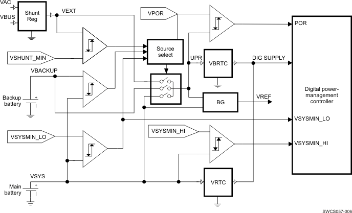 Figure 5-3 Block Diagram of the Analog Power Control
NOTE
- UPR = VSYS if: (VSYS > VSYSMIN_LO) or (VSYS > VBACKUP) and (VSHUNT < VSHUNT_MIN)
- UPR = VBACKUP if: (VSYS < VSYSMIN_LO) and (VSYS < VBACKUP – 0.1 V) and (VSHUNT < VSHUNT_MIN) and POR = 0
- UPR = VSHUNT if: (VSYS < VSYSMIN_LO) and (VSHUNT > VSHUNT_MIN)
Figure 5-4 shows the power state transition diagram.
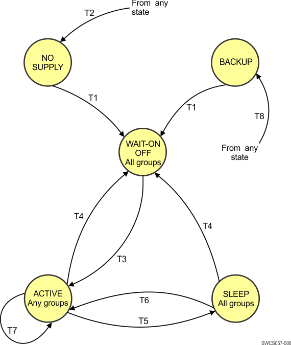 Figure 5-4 Power State Transition Diagram
- Power-on transitions: T1
- System is in NO SUPPLY or BACKUP state. Connection of a valid energy source initiates the transition to WAIT-ON state.
- Triggering event: VSYS > VSYSMIN_LO
- Insertion of a charged main battery
- Precharge is active main battery voltage rises
- Condition: VUPR > VPOR
- Power-off transition: T2
- The system is in any state. Removal of all energy sources initiates a transition to NO SUPPLY state.
- Triggering event: VUPR < VPOR
- Main battery discharge or removal
- Backup battery discharge or removal
- Charger unplugged
- Condition: No more valid energy source
- Switch-on transition: T3
- The system is in WAIT-ON state, able to accept a hardware switch-on condition, which initiates a transition to ACTIVE state.
- Triggering event:
- Push button pressed and released (PWRON)
- Charging source plug (USB or external)
- RTC alarm
- Accessory plug (RPWRON)
- Insertion of a charged main battery or battery charge running (enabled by default)
- Software reset (following transition T4)
- USB ID plug insertion (disabled by default)
- Condition: VSYS > VSYSMIN_HI and no thermal shutdown active
- Switch-off transition: T4
- System is powered and in ACTIVE or SLEEP state. A hardware condition may initiate a transition to reach WAIT-ON state.
- Triggering event:
- Group DEVOFF command (software)
- Thermal shutdown
- Primary watchdog timer expired
- Software reset (followed by transition T3)
- Long key press (8/4 seconds) on PWRON
- Sleep-on transition: T5
- System is powered and in ACTIVE state. A hardware condition initiates a transition to SLEEP state.
- Triggering event: Subsystem group sleep command (hardware) (PREQ1 ball)
- Sleep-off transition: T6
- System is powered and in SLEEP state. A hardware condition can initiate a transition to ACTIVE state.
- Triggering event:
- Subsystem group active command (hardware) (PREQ1 ball)
- Warm reset (reinitialization of the TPS80032 device)
- Active reset transition: T7
- System is powered and in ACTIVE state. A hardware condition can initiate a reset; system remains in ACTIVE state.
- Triggering event: Warm reset (reinitialization of the device)
- Backup-on transition: T8
- System is powered and in ACTIVE, SLEEP, or WAIT-ON state. The detection of a low main battery initiates the transition to BACKUP state.
- Triggering event: System voltage < VSYSMIN_LO (discharge/removal)
- Condition: VUPR > VPOR
5.6 System Voltage/Battery Comparator Thresholds
Three thresholds of battery voltage condition the system state transitions:
- POR
- Released when the energy source provides a voltage greater than 2 V
- POR threshold is the minimum voltage below which the TPS80032 device is reset.
- VSYSMIN_LO
- Threshold of hardware switch off
- Two values, depending on the battery technology, are stored in OTP memory (VSYSMIN_LO_MIN, VSYSMIN_LO_MAX bits) and selected by BOOT0 pin.
- The comparator threshold (VSYSMIN_LO) is configurable from 2.0 to 3.1 V in 50-mV steps.
- VSYSMIN_HI
- Threshold of switch on
- Checked as condition to initiate any sequence to ACTIVE state
- Two values, depending on the battery technology, are stored in OTP memory (VSYSMIN_HI_MIN, VSYSMIN_HI_MAX bits) and selected by BOOT0 pin.
- The comparator threshold (VSYSMIN_HI) is configurable from 2.5 to 4.6 V in 50-mV steps.
- For correct system behavior, the value of the VSYSMIN_HI threshold must not be programmed higher than the default system supply/charging voltage. Otherwise, the TPS80032 device does not switch on after a charger plug with empty battery.
NOTE
The system voltage must be above the VSYSMIN_HI threshold level in order to begin the start-up sequence. The TPS80032 device initiates the shut-down sequence if the system voltage decreases below VSYSMIN_LO. The dropout voltage requirements for the SMPSs and LDOs must be taken into account, otherwise the regulators may not fulfill their specifications.
5.7 Power Resources
The power resources provided by the TPS80032 device include inductor-based SMPSs and linear LDO voltage regulators. These supply resources provide the required power to the external processor cores and external components as well as to the modules embedded in the TPS80032 device.
5.7.1 Short-Circuit Protection
The short-circuit current limits for all LDOs and SMPS regulators embedded in the TPS80032 device are approximately twice their respective maximum load current. For specific LDO use cases, when the output of the module is shorted to ground, the power dissipation can exceed the power dissipation requirement, if no continuous preventive action is engaged.
The short-circuit protection scheme compares an LDO/SMPS output voltage to a reference voltage and detects a short circuit if the regulator voltage drops slightly below its minimum output voltage (1 V for LDOs and 0.6 V for SMPSs). A short-circuit protection scheme is included in each power resource of the TPS80032 device to ensure that if the output of an LDO or SMPS is short-circuited, the power dissipation does not increase drastically.
All LDOs/SMPSs include this short-circuit protection that monitors the regulator output voltage and generates an interrupt when a short-circuit is detected (see interrupt mapping). The VRTC regulator is the unique power resource that cannot generate an interrupt when shorted. Therefore, this regulator includes a different analog short-circuit mechanism that does not require a switch off the regulator.
If the short-circuit is detected the SMPS_LDO_SHORT_STS register is updated and the application processor needs to clear the short-circuit interrupt (VXXX_SHORT) and turn off the associated power resource within the 10-ms default time. If the interrupt is not cleared before the counter expires, the TPS80032 device switches off automatically. In parallel, the primary watchdog can shut down the device, if the watchdog expires.
In normal use conditions, when the TPS80032 device is turned off, all LDO/SMPS resources (except VRTC/VBRTC) are turned off and their corresponding short-circuit mechanisms are reset. If a short-circuit condition persists in which all power resources should normally be off, the TPS80032 device does not power up again.
CAUTION
If the external components of the SMPSs or LDOs are not placed and the regulator is enabled, the short-circuit detection triggers. If software is unable to clear the interrupt and shut down the regulator within the short-circuit counter time, the PMIC shuts down.
To generate a succesful start-up sequence, all the regulators enabled during start up must include the external components (capacitors and coils).
5.7.2 SMPS Regulators
The TPS80032 device includes five SMPS regulators, three of which have DVS capability and thus can be selected to provide independent core voltage domains to the host processor. Each SMPS is a high-frequency, synchronous, step-down DC-DC converter allowing the use of low-cost chip inductors and capacitors.
SMPS1 operates with a 3-MHz fixed-switching frequency and the other SMPSs operate at 6-MHz fixed-switching frequency and enters the power-save mode operation at light load currents to maintain high efficiency over the entire load current. Pulse-frequency modulation (PFM) mode extends the battery life by reducing the quiescent current to 30 µA (typical) during light load and standby operation. For noise-sensitive applications, the appropriate SMPS can be forced into fixed-frequency pulse-width modulation (PWM) mode (FORCE PWM setting in SMPSx_CFG_TRANS registers). In shutdown mode, the current consumption is reduced to less than 1 µA.
Each SMPS is a synchronous step-down converter operating with a fixed-frequency, PWM at moderate-to-heavy load currents. At light load currents, the converter operates in power-save mode with PFM. The converter uses a unique frequency locked-ring oscillating modulator to achieve best-in-class load and line response and allows the use of tiny inductors and small ceramic input and output capacitors. At the beginning of each switching cycle, the P-channel MOSFET switch is turned on and the inductor current ramps up, raising the output voltage until the main comparator trips. The control logic then turns off the switch.
One key advantage of the nonlinear architecture is the absence of a traditional feedback loop. The loop response to change in VO is essentially instantaneous, which explains its extraordinary transient response. The absence of a traditional, high-gain compensated linear loop means that the regulator is inherently stable over a wide range of L and CO. Each SMPS integrates a current limit in the P-channel MOSFET (in SMPS1 in the high-side N-channel MOSFET). When the current in the MOSFET reaches its current limit, the MOSFET is turned off and the low-side N-channel MOSFET is turned on for at least 150 ns.
With decreasing load current, the device automatically switches into pulse-skipping operation in which the power stage operates intermittently based on load demand. By running cycles periodically, the switching losses are minimized, and the device runs with a minimum quiescent current and maintains high efficiency. The converter positions the DC output voltage approximately 1% above the nominal output voltage. This voltage-positioning feature minimizes voltage drops caused by a sudden load step. When in PFM mode, the converter resumes its operation when the output voltage trips below the nominal voltage. It ramps up the output voltage with a minimum of three pulses and goes into PFM mode when the inductor current has returned to a zero steady state. Because of the dynamic voltage positioning, the average output voltage in PFM mode is slightly higher than its nominal value in PWM mode. During PFM operation, the converter operates only when the output voltage trips below a set threshold voltage. It ramps up the output voltage with several pulses and goes into PFM mode when the output voltage exceeds the nominal output voltage.
The rated output current is 5.0/3.0 A for SMPS1, 2.5 A for SMPS2, and 1.1 A for SMPS3, SMPS4, and SMPS5 regulators.
5.7.2.1 Soft Start
Each SMPS has an internal soft-start circuit that limits the inrush current and thus the input voltage drop during start up. The soft-start system progressively increases the on-time from a minimum pulse-width of 30 ns as a function of the output voltage. This mode of operation continues for 200 µs after enable. If the output voltage does not reach its targeted value by this time, such as in the case of heavy load, the soft-start transitions to a second mode of operation. The converter then operates in a current-limit mode, specifically the PMOS current limit is set to half the nominal limit and the N-channel MOSET remains on until the inductor current is reset. After an additional 100 µs, the device ramps up to full current-limit operation, providing that the output voltage rises above approximately 0.7 V. Therefore, the start-up time mainly depends on the output capacitor and load current.
5.7.2.2 Inductor Selection
All step-down converters are designed to operate with an effective inductance value from 0.40 to 1.30 µH and with output capacitors from 4 to 15 µF (15 to 29 µF for SMPS1 ). The maximum output capacitor value is normally used during the start-up phase, when the capacitor is still unbiased. The internal compensation is optimized to operate with an output filter of L = 1.0 µH and CO = 10 µF (SMPS2, SMPS3, SMPS4, and SMPS5) and CO = 22 µF (SMPS1 ). Larger or smaller inductor values can be used to optimize the performance of the device for specific operation conditions. If SMPS1 is used for up to 5.0-A current levels, it is recommended to use two 1.0-µH inductors in parallel.
The inductor value affects the following:
- The peak-to-peak ripple current
- The PWM-to-PFM transition point
- The output voltage ripple
- The efficiency
The selected inductor must be rated for its DC resistance and saturation current. The ripple current of the inductor decreases with higher inductance and increases with higher VI or VO.
In high-frequency converter applications, the efficiency is essentially affected by the inductor AC resistance (quality factor) and to a smaller extension by the inductor DCR value. To achieve high-efficiency operation, special care must be taken to select inductors featuring a quality factor above 20 at the switching frequency. Increasing the inductor value produces lower RMS currents, but degrades transient response. For a given physical inductor size, increased inductance usually results in an inductor with lower saturation current.
The total losses of the coil consist of the losses in the DC resistance and the following frequency-dependent components:
- The losses in the core material (magnetic hysteresis loss, especially at high switching frequencies)
- Additional losses in the conductor from the skin effect (current displacement at high frequencies)
- Magnetic field losses of the neighboring windings (proximity effect)
- Radiation losses
5.7.2.3 Output Capacitor Selection
SMPS advanced fast-response voltage mode control allows the use of tiny ceramic capacitors. Ceramic capacitors, with low ESR values, provide the lowest output voltage ripple. The output capacitor requires either an X7R or an X5R dielectric. Y5V and Z5U dielectric capacitors, aside from their wide variation in capacitance over temperature, become resistive at high frequencies.
At nominal load current, the device operates in PWM mode and the overall output voltage ripple is the sum of the voltage step caused by the output capacitor ESL and the ripple current flowing through the output capacitor reactance.
At light loads, the device operates in power-save mode, and the output voltage ripple is independent of the output capacitor value. The output voltage ripple is set by the internal comparator thresholds and propagation delays.
5.7.2.4 Input Capacitor Selection
Because the buck converter has a pulsating input current, a low ESR input capacitor must prevent large voltage transients that can cause misbehavior of the device or interferences with other circuits in the system. Although a 2.2-µF capacitor is sufficient for most applications, a 4.7-µF capacitor is recommended to improve input noise filtering.
CAUTION
Take care when using only ceramic input capacitors. When a ceramic capacitor is used at the input and the power is being supplied through long wires, such as from a wall adapter, a load step at the output can induce ringing at the VIN pin. This ringing can couple to the output and be mistaken as loop instability or could even damage the part. In this case, additional bulk capacitance (electrolytic or tantalum) must be placed between CI and the power source lead to reduce ringing that can occur between the inductance of the power source leads and CI.
5.7.2.5 SMPS1, SMPS2, SMPS5
The TPS80032 device includes three SMPS buck converters (SMPS1, SMPS2, and SMPS5) with DVS-control capability; their output voltages (SMPSx_CFG_FORCE registers) are independently controlled using the DVS-I2C dedicated interface. The output voltages can be also controlled using the CTL-I2C interface with SMPSx_CFG_VOLTAGE registers. Default output voltage at power up is configurable by the OTP memory. The regulators can be used, for example, for a processor or 1.8-V I/O supply.
SMPS1 has two output current ranges selectable by OTP memory bit (SMPS1_5A). A 3-A mode supports output currents up to a 3-A level and 5-A mode supports output currents up to a 5-A level. The electrical characteristics depend on the selected mode (see Table 4-1).
5.7.2.6 SMPS3, SMPS4
The TPS80032 device includes two SMPS buck converters (SMPS3 and SMPS4) that can be used, for example, for memory supply, peripheral, or preregulation.
5.7.3 LDO Regulators
All LDOs are integrated so that they can be connected to an internal preregulator, to an external buck boost SMPS, or to another preregulated voltage source.
The output voltages of all LDOs can be selected, regardless of the LDO input voltage level VIN. There is no hardware protection to prevent software from selecting an improper output voltage if the VIN minimum level is lower than TDCOV (total DC output voltage) + DV (dropout voltage). In such conditions, the output voltage would be lower and nearly equal to the input supply. For example, in further electrical tables, only the possible input supplies, which fulfill the electrical performances on all their range, are mentioned at each selected output.
The regulator output voltage cannot be modified on the fly, from the voltage range of 1.0 to 2.1 V to the other voltage range of 2.2 to 3.3 V and vice versa. The regulator must be restarted in these cases.
If an LDO is not needed and not turned on by software or a switch-on sequence, the external components can be removed. The TPS80032 device is not damaged by this configuration, and the other functions do not depend on the unmounted LDOs and continue to work.
5.7.3.1 VANA
The VANA voltage regulator is dedicated to supply the analog functions of the TPS80032 device, such as the GPADC, gas gauge, and other analog circuitries.
VANA can be enabled and disabled individually or when associated with a power group. This power resource control optimizes the overall SLEEP state current consumption. This regulator also can be used at platform level to supply other applications, provided they do not generate noise to the supply line and the maximum current is less than 15 mA.
5.7.3.2 VRTC, VBRTC
The VRTC voltage regulator supplies always-on functions, such as RTC and wake-up functions. This power resource is active as soon as a valid energy source is present.
This resource has two modes:
- Normal mode when supplied from main battery and able to supply all digital part of the TPS80032 device
- Backup mode when supplied from a backup battery or from weak main battery and able to supply only always-on parts
VRTC supplies the digital part of the TPS80032 device. In BACKUP state, the VRTC regulator is in low-power mode (VBRTC) and is supplied from backup battery or from weak main battery; the digital activity is reduced to the RTC parts only and maintained in retention registers of the backup domain. The rest of the digital is under reset and the clocks are gated.
In WAIT-ON state, the turn-on events and detection mechanism are also added to the previous RTC current load and are still supplied on VRTC or VBRTC (the supply is controlled with VRTC_EN_OFF_STS bit in BBSPOR_CFG register).
In ACTIVE state, by default the VRTC switches automatically into standard power mode (the supply is controlled with VRTC_PWEN bit in BBSPOR_CFG register). The reset is released and the clocks are available.
In SLEEP state, VRTC is kept active. The reset is released and only the 32-kHz clock is available. Still, to reduce power consumption, VBRTC instead of VRTC can be used by software (VRTC_EN_SLP_STS bit in BBSPOR_CFG register).
5.7.3.3 LDO1, LDO2, LDO3, LDO4, LDO5, LDO6, LDO7
LDO5 is a programmable linear voltage converter used to power, for example, a multimedia card (MMC) slot. On top of the normal control by the power controller, it can be turned off when card removal is detected (the LDO5_AUTO_OFF bit in the MMCCTRL register).
Voltage regulator LDO7 can be used to supply removable USIM memory. In addition to the normal control by the power controller, it can be turned off when card removal is detected (the VSIM_AUTO_OFF bit in the SIMCTRL register).
The TPS80032 device includes five general-purpose resources (LDO1, LDO2, LDO3, LDO4, and LDO6) to supply external peripherals, such as cameras sensors, display drivers, memories (eMMC), and others. When not used as a supply, LDO3 can deliver a PWM supply to drive a vibrator motor.
5.7.3.4 LDOLN, LDOUSB
The LDOLN regulator supplies noise-sensitive functions. LDOLN can be preregulated by SMPS.
The LDOUSB regulator supplies the USB PHY from the PMID node of the USB VBUS input or from system supply/battery.
5.8 Backup Battery Charger
The TPS80032 device provides a BACKUP state in which a backup battery powers the RTC and other secure registers when no other energy source is available. The backup battery is optional and can be nonrechargeable or rechargeable. The rechargeable battery can be charged from the system supply using the backup battery charger.
The backup battery charger includes two control loops (CC and CV). A current loop limits the charging current when backup battery voltage is low and a voltage loop that gradually reduces the charging current as backup battery voltage approaches its final value. The charge current limit is fixed and the end of charge voltage is programmable (BB_SEL[1:0] bits in BBSPOR_CFG register).
The backup battery charger is controlled with BB_CHG_EN bit (in BBSPOR_CFG register) and the charging starts if the system supply voltage is 100 mV above backup battery voltage; charging stops when backup battery voltage equals either the selected end of charge voltage level or the system supply voltage, if it is below the end of the charge level programmed. Backup battery charge cannot start if system supply voltage is lower than VSYSMIN_LO. The backup battery switch controls when the system enters BACKUP state (supplied by the backup battery).
During the transition from system supply to backup battery there can be a current spike from the backup battery. If the output resistance of the backup battery is large, an additional capacitor is needed in parallel with the backup battery. See the electrical characteristics for more details.
Figure 5-5 shows a block diagram of the backup battery charger.
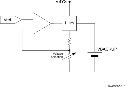 Figure 5-5 Block Diagram of the Backup Battery Charger
5.9 Battery Charging
The TPS80032 device has an integrated switched-mode battery charger designed to generate a system supply and to charge the battery from a USB port. In addition, it can control an external battery charging IC (like BQ24159) to generate a system supply and charge the battery during hardware-controlled charging and selects the priority of the chargers so that only one is enabled at time.
Figure 5-6 shows the block diagram of the USB charging electronics. The figure shows the USB charging-related functions with external components. The device supports two charging configurations, operation with Power Path and without Power Path.
In the Power Path configuration the battery line is connected to the system supply with external PMOS transistor. The system supply is regulated by switched-mode regulator and the battery charging current and voltage are controlled with a battery charger loop and external PMOS transistor. The sense resistor at the output of switched-mode regulator is not needed. When the platform is supplied by battery the external PMOS is closed.
In the non-Power Path configuration the battery line is used as a system supply and the external PMOS is not needed because the battery current is monitored with a resistor placed between ground and negative terminal of the battery. In this configuration a sense resistor at the output of the switched-mode regulator is needed as it is used to control the battery charging current.
For information about the functions and external components related to VAC charging, see Section 5.9.12, Support for External Charging IC.
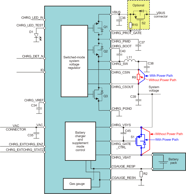 Figure 5-6 Block Diagram of the System Supply Regulator and Battery Charger
The TPS80032 device supports a wide variety of rechargeable lithium-based battery technologies. Recent battery technologies, such as Li-SiAn and LiFePo4, present a flat discharge region in the range of 3.2–3.3 V; technologies such as LiCoO2 and LiNiMnCoO2 present a flat discharge region in the range of 3.6–3.7 V. To support the different battery chemistries effectively, the TPS80032 device has programmable VSYSMIN thresholds (OTP bits).
The charger also performs monitoring functions:
- AC charger detection
- VBUS detection
- Battery presence detection
- VBUS overvoltage detection
- Battery overvoltage detection
- Battery end-of-charge detection
- Thermal protection
- Watchdogs
The same switches and external components that are used for system supply generation in buck mode can be used to generate a 5-V USB OTG supply in boost mode. In this mode, the TPS80032 device can deliver up to 300 mA of total current for USB connector and for LDOUSB.
The VBUS input in the TPS80032 device operates up to 6.3 V; above this, level the system supply regulator is disabled. The VBUS input tolerates up to 20-V input voltages and down to –0.3-V input voltages. The negative input voltage protection can be improved with external PMOS transistor and resistor (shown in Figure 5-6 as optional components). This gives tolerance down to –14 V.
NOTE
The charging source terms are defined as follows (USB Battery Charging Specification, Rev. 1.2)
- Standard Downstream Port (SDP): a downstream port on a device that complies with the USB 2.0 definition of a host or hub.
- Charging Downstream Port (CDP): a downstream port on a device that complies with the USB 2.0 definition of a host or a hub, except that it shall support the Charging Downstream Port features allowing higher charging currents.
- Dedicated Charging Port (DCP): a downstream port on a device that outputs power through a USB connector, but is not capable of enumerating a downstream device.
- USB Charger: a device with a DCP, such as a wall adapter or car power adapter.
- Accessory Charger Adaptor (ACA): an adaptor which allows a single USB port to be attached to both a charger and another device at the same time.
- Charging Port: a DCP, CDP or ACA
5.9.1 Charger and System Supply Regulator Controller Operation
The operation of the battery charger and the system supply regulator depends on the platform configuration. There are two different configurations for hardware:
- Power Path configuration (POP_APPSCH OTP bit is 1); an external PMOS is needed between VSYS and VBAT.
- Non-Power Path configuration (POP_APPSCH OTP bit is 0); VBAT is used as a system voltage.
In addition, software interaction with battery charging in both configurations depends on the AUTOCHARGE OTP bit:
- Hardware controlled charging (AUTOCHARGE bit is 1); software interaction is minimized.
- Software controlled charging (AUTOCHARGE bit is 0); software controls the battery charging.
The operation in the four different modes has been described in Section 5.9.1.1 through Section 5.9.1.4. The flow chart for startup, shutdown, and fallback (Power Control) operates in parallel with a flow chart of the system supply regulator and battery charging (Charger Control). The safety timer and watchdog operation is described in Section 5.9.6 and the charging profile and default charging parameters are described in Section 5.9.3.
5.9.1.1 Power Path with Hardware Controlled Charging
The TPS80032 device starts up for the VBUS or VAC plug insertion as soon as the system voltage is above the VSYSMIN_HI threshold level if the device is not already powered on. The hardware starts the system supply regulation and battery charging automatically if a USB Charging Port or VAC Charger is detected, or if the battery voltage is below VBATMIN_HI and the device is powered off. If the VBUS is supplied by the USB standard downstream port and the battery is above VBATMIN_HI or the device is powered on, the system supply regulator and battery charger are not started by hardware. The host processor must enumerate to the USB host, configure to a certain current level, set the VBUS input current limit, and enable the system supply regulator and battery charging.
If the system voltage drops below VSYSMIN_LO, the device shuts down and sets a fallback bit to indicate the fallback situation. A new startup is initiated when the battery is charged above the VBATMIN_HI voltage level and after startup, the host processor clears the bit. If the fallback bit is active during the shutdown, the system supply regulator and battery charging is disabled. This prevents infinite looping in a low/no battery case with a weak charger. The operation is shown in Figure 5-7.
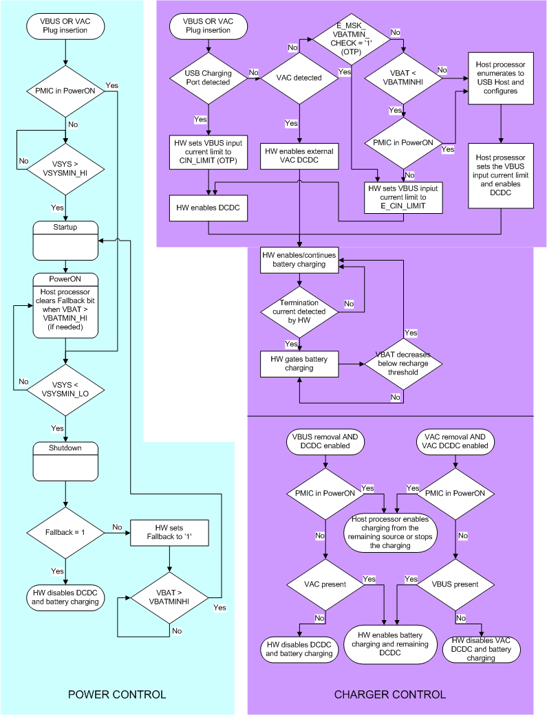 Figure 5-7 Battery Charging Flowchart (With Power Path, AUTOCHARGE=1)
5.9.1.2 Power Path with Software Controlled Charging
The TPS80032 device starts up for the VBUS or VAC plug insertion as soon as system voltage is above the VSYSMIN_HI threshold level if the device is not already powered on. If the device is powered off, the hardware sets the correct VBUS input current limit and starts the system supply regulator either from VBUS or from VAC and the battery charging using the default values from OTP memory. The default charging voltage must be set to the proper battery threshold voltage level to comply with the USB standard. When the device is powered on, the host processor takes control over charging.
If the system voltage drops below VSYSMIN_LO, the device shuts down and sets a fallback bit to indicate the fallback situation. A new startup is initiated when the battery is charged above the VBATMIN_HI level and the host processor clears the bit. If the fallback bit is active during the shutdown, the system supply regulator and battery charging is disabled. This prevents infinite looping in a low/no battery case with a weak charger. The operation is shown in Figure 5-8.
 Figure 5-8 Battery Charging Flowchart (With Power Path, AUTOCHARGE=0)
5.9.1.3 Non-Power Path with Hardware Controlled Charging
The TPS80032 device starts up for the VBUS or VAC plug insertion as soon as battery voltage is above the VSYSMIN_HI threshold level if the device is not already powered on. The hardware starts the battery charging automatically if USB Charging Port or VAC Charger is detected, or if the battery voltage is below VBATMIN_HI and the device is powered off. If the VBUS is supplied by the USB standard downstream port and the battery voltage is above VBATMIN_HI or the device is powered on, the battery charger is not started by hardware. The host processor must enumerate to the USB host, configure to a certain current level, set the VBUS input current limit, and enable the battery charging.
If the battery voltage drops below VSYSMIN_LO, the device shuts down and sets a fallback bit to indicate about the fallback situation. A new startup is initiated when the battery is charged above the VSYSMIN_HI threshold level and after startup the host processor clears the bit. If the fallback bit is active during shutdown, the battery charging is disabled. This prevents infinite looping in low/no battery case with weak charger. The operation is shown in Figure 5-9.
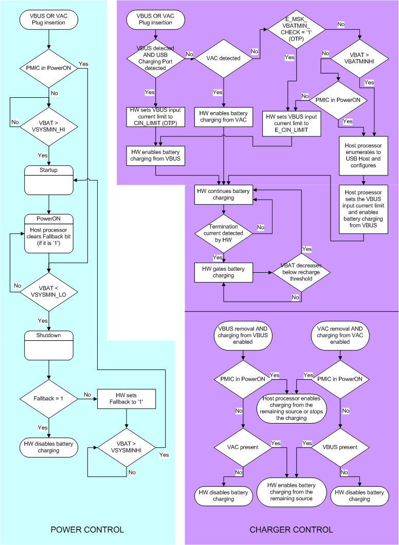 Figure 5-9 Battery Charging Flowchart (Without Power Path, AUTOCHARGE=1)
5.9.1.4 Non-Power Path with Software Controlled Charging
The TPS80032 device starts up for the VBUS or VAC plug insertion as soon as battery voltage is above the VSYSMIN_HI threshold level if the device is not already powered on. If the device is powered off, the hardware sets the correct VBUS input current limit and starts the battery charging using the default values from OTP memory. The default charging voltage need to be set to good battery threshold voltage level in order to comply with the USB standard. When the device is powered on, the host processor takes control over charging.
If the battery voltage drops below VSYSMIN_LO, the device shuts down and sets a fallback bit to indicate the fallback situation. A new startup is initiated when the battery is charged above the VSYSMIN_HI threshold level and the host processor clears the bit. If the fallback bit is active during the shutdown, the battery charging is disabled. This prevents infinite looping in a low/no battery case with a weak charger. The operation is shown in Figure 5-10.
 Figure 5-10 Battery Charging Flowchart (Without Power Path, AUTOCHARGE=0)
5.9.2 System Supply Regulator
During software-controlled charging, software selects the VBUS input current limit, the VBUS input voltage collapse level, and the system supply regulation voltage. The programmable resources are:
- Input limit current set point register CIN_LIMIT[3:0] (maximum current drawn from VBUS charging source)
- Input voltage set point register BUCK_VTH[2:0] (VBUS voltage collapsing level)
- System supply voltage set point register
The system supply regulation voltage can be a fixed voltage or follow the battery voltage allowing the linear battery charger to regulate the charging current and voltage (DPPM control mode).
5.9.3 Battery Charging
5.9.3.1 Power Path Configuration
When the Power Path configuration is used, the battery charging consists of two different regulators, the system supply regulator generating the system supply (VSYS) from the USB VBUS voltage and a linear battery charging loop regulating the battery node (VBAT) from the system supply (VSYS) using an external PMOS transistor. During the preconditioning phase, an integrated current source is used for battery charging. The use of the dedicated loop for battery charging allows monitoring of the battery current and voltage independently and minimizes the power dissipation thanks to the low-ohmic external transistor.
The TPS80032 device includes five analog loops that influence the system supply regulator's output current:
- System voltage regulation loop, maintaining the system voltage (VSYS) at constant level (VSYS_PC) during preconditioning and precharging and at (VBAT+DLIN[1:0]) level during full-charge phase and end-of-charge phase.
- VBUS voltage anticollapse loop sensing the VBUS voltage and preventing the VBUS voltage from dropping below the programmed level (BUCK_VTH[2:0]).
- VBUS input current loop sensing the input current and limiting it below the programmed level (CIN_LIMIT[5:0]).
- Thermal regulation loop sensing the DCDC temperature and limiting it below thermal shutdown level.
- Cycle-by-cycle current monitoring loop sensing the current in high-side switch and limiting it below cycle-by-cycle limit (BUCK_HSLIMI).
The dedicated battery charging control includes three loops that influence the battery charging current:
- Constant current (CC) loop sensing the battery current and limiting it below charging current level (VICHRG[3:0]).
- Constant voltage (CV) loop sensing the battery voltage and limiting it below charging voltage level (VOREG[5:0]).
- DPPM loop monitoring the voltage between system voltage and battery voltage and limiting the voltage to threshold level (DLIN[1:0]/2) by decreasing the charging current.
Figure 5-11 shows the control loops for the system supply regulation and for the battery charging.
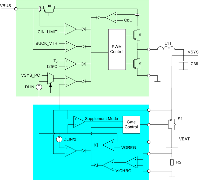 Figure 5-11 System Supply Regulator and Battery Charging Control Loops
CAUTION
Resistor R2 is used for charging current control in Power Path configuration and must be placed even if Gas Gauge is not used.
In addition, a battery current is monitored and if the termination current level (VITERM[2:0]) is detected an interrupt is generated and battery charging is stopped according to the selected operation.
The battery charging profile consists of three phases:
- Preconditioning
- Precharging
- Full-charge phase
NOTE
The DLIN[1:0] voltage level must be selected so that the voltage is higher than the maximum dropout on the switch (maximum charging current multiplied by the maximum resistance of the switch).
Figure 5-12 shows a charging profile and the different parameters programmed in OTP memory and software programmable parameters for charging with Power Path. The charging current is usually limited by the VBUS input current loop when charging from the standard downstream port because the limit is set to 100 or 500 mA. If the charging source cannot provide the current the charger is drawing, the VBUS voltage decreases. The VBUS anticollapse loop senses the VBUS voltage and decreases the current so that the voltage does not fall below the programmed voltage level (see Section 5.9.4).
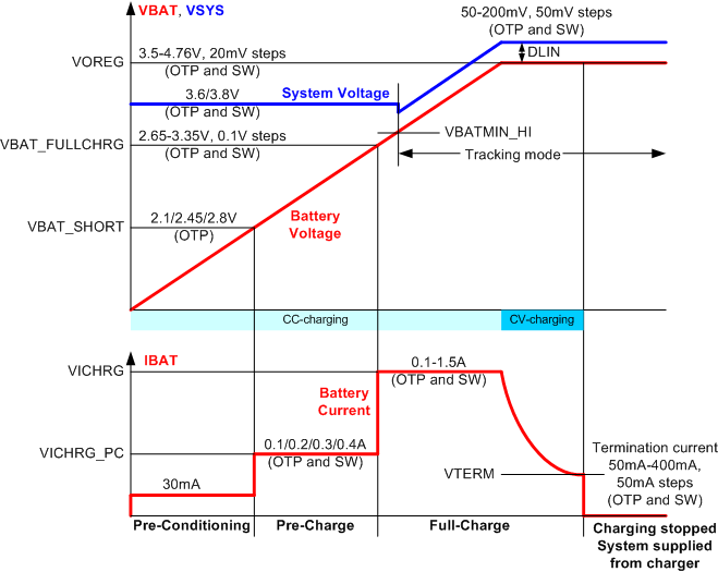 Figure 5-12 Battery Charging Profile with Power Path (Resistor R2 = 20 mΩ)
5.9.3.2 Non-Power Path Configuration
When the non-Power Path configuration is used, the battery charging is controlled by switched-mode regulator from the USB VBUS voltage.
The TPS80032 device includes six analog loops that influence the output current:
- VBUS voltage anticollapse loop sensing the VBUS voltage and preventing the VBUS voltage from dropping below the programmed level (BUCK_VTH[2:0]).
- VBUS input current loop sensing the input current and limiting it below the programmed level (CIN_LIMIT[5:0]).
- Constant voltage (CV) loop sensing the battery voltage and limiting it below charging voltage level (VOREG[5:0]).
- Constant current (CC) loop sensing the battery current and limiting it below charging current level (VICHRG[3:0]).
- Cycle-by-cycle current monitoring loop sensing the current in high-side switch and limiting it below cycle-by-cycle limit (BUCK_HSLIMI).
- Thermal regulation loop sensing the DCDC temperature and limiting it below thermal shutdown level.
Figure 5-13 shows the control loops for the battery charging.
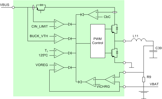 Figure 5-13 Battery Charging Control Loops.
In addition, a battery current is monitored and if the termination current level (VITERM[2:0]) is detected an interrupt is generated and battery charging is stopped according to the selected operation.
The battery charging profile consists of three phases:
- Preconditioning
- Precharging
- Full-charge phase
Figure 5-14 shows a charging profile and the different parameters programmed in OTP memory and software programmable parameters for HW controlled operation (AUTOCHARGE=1) and Figure 5-15 shows a charging profile and the different parameters programmed in OTP memory and software programmable parameters for SW controlled operation (AUTOCHARGE=0). The charging current is usually limited by the VBUS input current loop when charging from the standard downstream port because the limit is set to 100 or 500 mA. If the charging source cannot provide the current the charger is drawing, the VBUS voltage decreases. The VBUS anticollapse loop senses the VBUS voltage and decreases the current so that the voltage does not fall below the programmed voltage level (see Section 5.9.4).
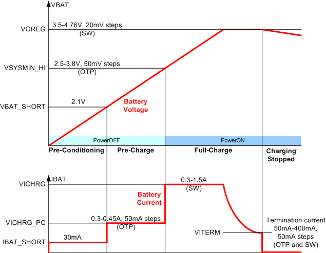 Figure 5-14 Battery Charging Profile Without Power Path (AUTOCHARGE=1, Resistor R9 = 68 mΩ)
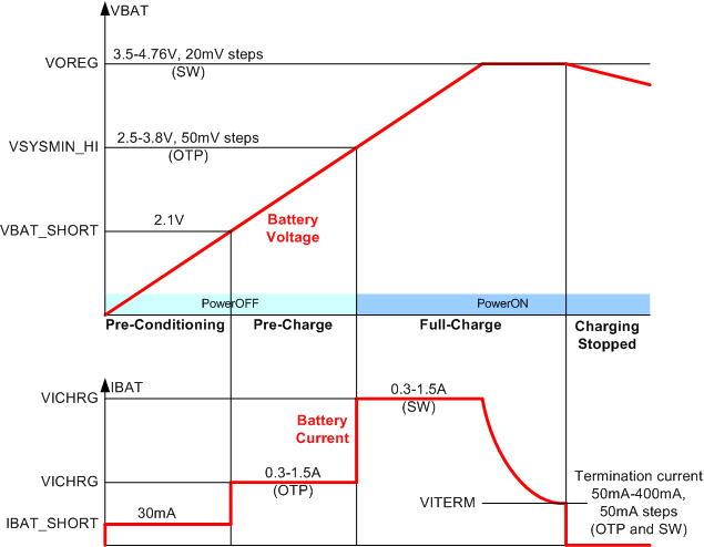 Figure 5-15 Battery Charging Profile Without Power Path (AUTOCHARGE=0, Resistor R9 = 68 mΩ)
5.9.3.3 Preconditioning
During preconditioning, the battery voltage is below the VBAT_SHORT level and the charging current is limited to 30 mA (IBAT_SHORT). If the system supply in Power Path configuration decreases during the preconditioning phase, the preconditioning current is automatically reduced. In this mode, the charger uses a linear charging operation mode. This phase detects a defective (shorted) battery and brings the battery voltage to a level acceptable for higher charging current. If the battery is defective (shorted) and the battery voltage doesn't increase above VBAT_SHORT level the charger stays in preconditioning phase. As soon as the battery voltage is above VBAT_SHORT, a precharging phase is entered automatically. In Power Path configuration the VBAT_SHORT level is programmed by OTP memory (VBAT_SHORT[1:0] bits).
5.9.3.4 Precharge Phase
The precharging phase is used when the battery voltage is between VBAT_SHORT and VBAT_FULLCHRG (VSYSMIN_HI without Power Path). If the system supply in Power Path configuration decreases during the precharge phase, the precharge current is automatically reduced (DPPM loop). During precharging, the charging current is limited to decrease the power dissipation in the external PMOS. The precharging current is programmed in OTP memory (VICHRG_PC[1:0] bits).
The precharge current level is controlled by monitoring the voltage across the sense resistor. The default currents are available with resistor R9 = 68 mΩ without Power Path and R2 = 20 mΩ with Power Path.
5.9.3.5 Full-Charge Phase
The full-charge phase starts when the battery voltage is above VBAT_FULLCHRG and the system supply is regulated from a charging source (without Power Path, the threshold level is VSYSMIN_HI).
With Power Path, the transition from a fixed system supply level into a tracking system supply level is done when the battery voltage is at the VBATMIN_HI level. The VBATMIN_HI level is the same as VSYSMIN_HI level (defined by OTP memory bits, VSYSMIN_HI[5:0]) except that the level is limited to 3.7 V. This means that if the VSYSMIN_HI is programmed above the 3.7-V level, the transition is done at the 3.7-V level. VBATMIN_HI is defined in the VBATMIN_HI_THRESHOLD register and the host processor can change the level. The threshold is updated with the default value from OTP memory during startup.
If the system voltage decreases during the full-charge phase, the charging current is automatically reduced (DPPM loop) to a value keeping the dropout voltage higher than 50% of the dropout voltage setting (programmed with the DLIN[1:0] bits in the CONTROLLER_VSEL_COMP register), to ensure proper operation of the charging circuitry.
The full-charge current level is controlled by monitoring the voltage across the sense resistor. The default currents are available with resistor R9 = 68 mΩ without Power Path and R2 = 20 mΩ with Power Path.
5.9.3.6 Termination Current Detection
The battery current is monitored during CV-charging and if the termination current level is triggered in the Power Path configuration, the battery charging is gated but the system voltage regulation from the VBUS input continues. If the battery voltage decreases 120 mV below the charging voltage (VOREG) level, the full-charge phase is continued.
In the non-Power Path configuration the operation during termination current level detection is defined by the CHARGE_ONCE and TERM bits. If the CHARGE_ONCE bit is 1, the battery charging is terminated when the termination current threshold is triggered. If the CHARGE_ONCE bit is 0 and TERM bit is 1, the battery charging is gated when the termination current level is triggered. If the battery voltage decreases 120 mV below the charging voltage (VOREG) level, the full-charge phase is continued.
The termination current level is monitored by measuring the voltage across the sense resistor. The default currents are available with resistor R9 = 68 mΩ without Power Path and R2 = 20 mΩ with Power Path.
5.9.4 Anticollapse Loop and Supplement Mode
There are two different anticollapsing loops; one monitoring the VBUS input and controlling the switched-mode regulator and another one with Power Path operation (DPPM) monitoring the VSYS line and controlling the linear battery charger loop.
The anticollapse loop of the VBUS input operates so that the VBUS input voltage is monitored continuously and the current of the switched-mode regulator is controlled by an analog loop to maintain the defined VBUS input voltage (programmed with the BUCK_VTH[2:0] bits in the ANTICOLLAPSE_CTRL1 register). If the VBUS source cannot deliver high enough current and the VBUS voltage drops, the VBUS input current is decreased by the analog loop so that the VBUS voltage stays at programmed level. If an external PMOS is used to protect the VBUS input against negative voltage, then the VBUS voltage at the connector can be slightly different because the anticollapse loop monitors the voltage at the PMIC input.
The anticollapse loop of the linear battery charger (DPPM) monitors the system voltage (VSYS) and controls the battery charging current. If battery voltage is below the VBATMIN_HI the threshold, the level for the DPPM loop is 3.4 V, whereas if the battery voltage is above VBATMIN_HI, the VSYS voltage tracks the VBAT voltage and the DPPM threshold is 50% of the programmed tracking voltage.
Figure 5-16 shows an example of DPPM loop and supplement mode operation. The charging current is set to 1 A and the VBUS input current limit is 1.5 A. When the system load is small the 1000 mA charging current can be generated with around 750 mA VBUS current, thanks to the efficient DCDC converter. If the system load is increased to around 900 mA level, the 1500 mA VBUS input current limit is reached and the DPPM loop decreases the battery charging current in order to maintain 50% of the programmed tracking voltage across the external FET. If the system load is increased further up to around 1900 mA level, the battery charging current decreases to 0 mA and the supplement mode is enabled. Increasing the system load above 1900 mA level directly affects the battery discharge current level. When the system load is decreased the operation is opposite entering from supplement mode into DPPM loop operation and finally out from VBUS input current limit mode.
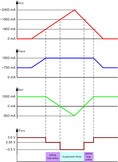 Figure 5-16 Example of DPPM Loop and Supplement Mode Operation (VVBUS = 5 V, VBAT = 3.5 V, 1.5 A VBUS Input Current Limit)
5.9.5 Battery Temperature Monitoring
JEITA requirements define the maximum battery charging current and voltage at different temperature ranges for Li-Ion batteries. The TPS80032 device supports the JEITA requirements with hardware-based temperature measurement gating the battery charging below and above the preset temperature values (typically 0°C and 60°C). Between these limits host processor must monitor the battery temperature using the integrated general-purpose analog-to-digital converter (GPADC) and setting the charging current and voltage accordingly. Figure 5-17 shows the voltage and current limits at different temperatures.
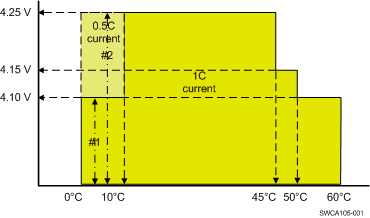 Figure 5-17 Charging Current and Voltage Limits at Different Temperatures
Figure 5-17 allows two options for charging between 0°C and 10°C. As shown in the figure, #1 allows charging up to 4.10 V with 1C current and #2 allows charging up to 4.25 V with 0.5C current. The term 1C defines the charging current related to the battery capacity. For a 1200-mA-h battery 1C corresponds to a 1.2-A current.
The battery temperature is measured using an external NTC resistor. The measurement is enabled before the charging starts and the temperature is constantly monitored during charging. If the battery temperature is outside of the valid range, the charging is gated; if the temperature returns to the valid range, the charging continues. In Power Path mode the system supply regulation is continued when the battery charging is gated. The gating of the charging can be disabled with an OTP memory bit (EN_BAT_TEMP) if needed. The temperature measurement circuitry is enabled if VBUS or an external charger is detected. An interrupt (CHRG_CTRL) is always generated when the battery temperature crosses the temperature limits in both directions. The interrupt generation can be masked if needed.
Figure 5-18 shows the battery temperature measurement circuitry.
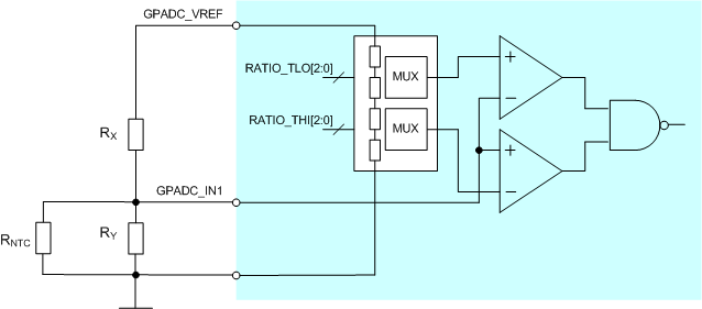 Figure 5-18 Battery Temperature Measurement
Because the NTC characteristics are highly nonlinear, it is combined with two resistors allowing linearization of its characteristics and making the sensitivity of the system more constant over a wide temperature range. The resulting voltage at GPADC_IN1 can be measured using the GPADC and is also monitored by two comparators that enable the charge of the battery only when the temperature is within a specified window, typically 0°C to 60°C. Resistors RX and RY are used to set the desired temperature threshold levels.
5.9.6 Safety Timer and Charging Watchdog
The TPS80032 device includes a safety timer, the timing of which depends on the charging control mode and the USB Charging Port detection result. During hardware-controlled charging, the period for the USB charging port and the USB standard downstream port is approximately 6 minutes; for customer-specific chargers, this period is approximately 14 minutes. Longer values can be selected with the OTP memory (CHWDT_DEP0 bit), 11 minutes instead of 6 minutes and 29 minutes instead of 14 minutes. Charger source dependency on the timer values can be enabled and disabled by OTP memory (CHWDT_DEP_DETN bit). If disabled, the timer value is always set as for the USB standard downstream port and for the customer-specific charger (longer timer value). During software-controlled charging the safety timer is replaced by charging watchdog (SW WDT), host processor can select the watchdog time up to 127 seconds. The transition from safety timer to software-controlled watchdog occurs when software updates the WDG_RST, WDT[6:0], VICHRG[3:0], VOREG[5:0] bits or CONTROLLER_CTRL1 register. The different safety timer and watchdog times are summarized in the EPROM bits Application Note. If the AUTOCHARGE mode is selected by OTP memory bit, the fixed 8-hour watchdog (HW WDT) is taken into use when the battery voltage is above the VBATMIN_HI level.
If the safety timer or watchdog expires, the battery charging is gated and interrupt is sent to host processor. In Power Path configuration, the system supply regulator still continues to operate when the battery charging is gated.
The operation of the safety timer and watchdog is presented in Figure 5-19.
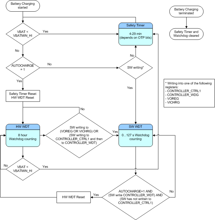 Figure 5-19 Safety Timer and Charging Watchdog
5.9.7 Limit Registers
During the full-charge phase, host processor sets the charging voltage and current. However, the device limits the current and voltage to a level that is defined in the limit registers (CHARGERUSB_CTRLLIMIT1 and CHARGERUSB_CTRLLIMIT2). The limit registers in the device must be written just after the startup. Host processor must check the battery type and define the maximum charging current and voltage for the battery being used, write the limit values, and lock the limit registers with the LOCK_LIMIT bit, so that these cannot be changed when the device is powered on. This ensures that third-party software or a virus cannot set a charging current or voltage that is too high. The limit values are reset during power off by the NRESPWRON signal and they must be written by host processor during every power up. Figure 5-20 shows the structure of the limit and programming registers.
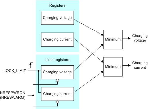 Figure 5-20 Charging Current and Voltage Limit Registers
5.9.8 Battery Presence Detector
The TPS80032 device supports battery detection. The presence of the battery can be detected with the GPADC_IN0 input signal. The interface has two different functions:
- Detect battery removal and presence
- Measure the size of the resistor connected to the GPADC_IN0 line in the battery pack using the GPADC
Battery pack removal is detected by a comparator that monitors GPADC_IN0. The battery pack must have a pull-down resistor (RBRI) and the device has a current source (IBRI) in the line. If the battery pack is removed, GPADC_IN0 rises above the comparator threshold level, the battery removal is detected, and the device sends an indication (BAT interrupt) to the host processor. In addition, battery charging is terminated if the battery is not present. Battery removal is detected with a comparator and a current source supplied on the VRTC supply domain. This supply scheme allows detection in a dead battery case configuration, because the VRTC can be supplied from the VBUS or VAC lines. The battery presence detection module is enabled during the charging and during the ACTIVE and SLEEP states.
Figure 5-21 shows a block diagram of the battery presence detection circuitry.
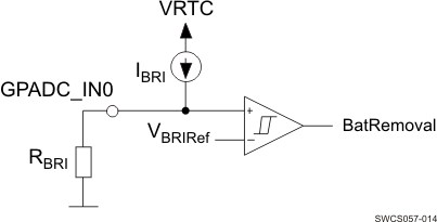 Figure 5-21 Battery Presence Detector
CAUTION
If the GPADC_IN0 line is not used for battery presence detection in the Power Path configuration (POP_APPSCH OTP bit is 1), the capacitance of the VBAT line must be below 100 µF. Otherwise a fully discharged battery cannot be detected correctly by the battery charging loop.
5.9.9 Indicator LED Driver
The device has an indicator LED driver that indicates charging is ongoing during hardware-controlled charging. During hardware-controlled charging, the LED driver is enabled only if the charging is ongoing and it is turned off if the battery is not charged. The supply for the charging indicator LED driver is generated from CHRG_PMID or VAC, depending on the active charging path. The CHRG_PMID pin is used instead of the VBUS line so that the LED indicator current is included into the VBUS input current limit.
During power on, host processor can control the indicator LED regardless of the charging with register bits (LED_PWM_CTRL1 and LED_PWM_CTRL2). The supply for the LED can be selected as CHRG_PMID, VAC, or CHRG_LED_IN. The current level can also be selected and the dimming function can be used. Dimming is done with a 128-Hz PWM signal, which has 255 linear steps. The LED output pin has a selectable pulldown when the module is disabled; the pulldown is enabled by default.
The indicator LED driver is also used to indicate if the device cannot power on after a key press (PWRON). If the battery voltage is too low for startup, the LED driver gives three 300-ms pulses with a 300-ms duration between the pulses.
5.9.10 Supported Charging Sources
The following chargers are supported with the integrated switched-mode charger from the USB connector:
- Dedicated Charging Port (DCP)
- Charging Downstream Port (CDP)
- Standard Downstream Port (SDP)
- Chinese charger
To configure the system supply regulator and charger for proper operation mode depending on the charging source characteristics, the charging source type must be detected and identified. The detection of the charger attached to the USB connector is made inside the device by detecting a voltage greater than VINmin on the charger input.
To minimize the capacitance of the data lines, the type of the charger connected to the USB connector can be identified by the USB PHY and the information of the maximum current drawn from the charging source can be transmitted to the device with a dedicated signal (CHRG_DET_N). The TPS80032 device enables detection by delivering the LDOUSB supply (selectable by OTP memory bit, AUTO_LDOUSB_DIS). The charger detection circuitry must deliver at least a 1.8-V voltage level to the CHRG_DET_N input pin, by default a high logic level indicating that a USB charging port is detected. The polarity of the charger detection signal can be selected with an OTP memory (DET_N_POL bit). The accessory charger adapter (ACA) is identified in the TPS80032 device. A typical connection of the PMIC and USB PHY is shown in Figure 5-22.
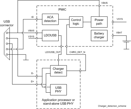 Figure 5-22 Connection for the USB Charging Port Detection
The device can be interfaced with an ACA (external to the terminal) to support charging from the USB Charging Port and USB communication to other USB devices from the USB port. For a description of ACA detection, see USB OTG, USB OTG.
5.9.11 USB Suspend
The TPS80032 device includes a HZ_MODE bit which is usable, for example during USB suspend periods. The benefit of the bit is that it can be used to gate the charging without changing any charging parameters. When the suspend period ends, clearing the bit continues the battery charging.
5.9.12 Support for External Charging IC
The TPS80032 device can be interfaced with an auxiliary stand-alone charger device to support the following use cases:
- Simultaneous battery charging from other than USB connector (different connector) and OTG operating mode with USB connector (the integrated switched-mode system supply regulator used as the VBUS supply)
- System supply generation and charging from the sources not connected to the USB connector
In the Power Path configuration the battery charging is always controlled by the TPS80032 device and the external IC only generates the system supply which is needed for the battery charging. In the non-Power Path configuration the external IC is used for battery charging. Figure 5-23 shows the connections between TPS80032 device, application processor and external charging IC (BQ24159) in Power Path configuration.
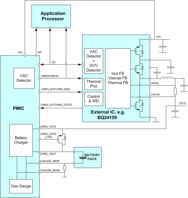 Figure 5-23 Connection Diagram for External Charging Interface in Power Path Configuration
The external IC is enabled with a 1.8-V CMOS level signal, CHRG_EXTCHRG_ENZ. A low logic level indicates that the regulator is enabled. The system supply regulation / battery charging status is indicated with the CHRG_EXTCHRG_STATZ signal. An external IC pulls the signal down during operation.
The integrated USB regulator can be associated with an external VAC regulator. For that reason, the VAC wall charger input is connected to the device to define the priorities. These priorities are controlled by hardware when the device is powered off (NRESPWRON=0):
- When the VBUS is detected and the VAC is not detected, the USB input is used.
- When the VAC is detected and the VBUS is not detected, the external charging input (VAC) is used.
- When the VBUS and VAC are detected:
- If CHRG_DET_N = 0 and ACA (RID_A, RID_B or RID_C) is not detected (100-mA VBUS input current limit), the VAC wall charger is expected to be better (or equivalent) and thus is chosen as the default input path.
- If CHRG_DET_N = 1 or ACA (RID_A, RID_B or RID_C) is detected (USB Charging Port detected), the USB is expected to be sufficient for system supply generation and charging and thus is chosen as the default input path.
If there is a fault condition on a charger during hardware-controlled operation and the fault condition continues for at least 2.5 seconds, the input source is changed for a lower priority input. The change into a lower priority input only prevents infinite looping between inputs. If only one charger is attached, the regulator is not disabled in a fault condition, and if the fault condition does not disappear; the input is terminated when the watchdog expires.
NOTE
In the Power Path mode the system voltage level is regulated according to the voltage level set in the BQ24159. There is no automatic tracking of the battery voltage like when integrated DCDC is used for system supply regulation. The voltage tracking must be done by host processor in order to maintain high enough dropout for the external PMOS transistor and on the other hand to limit the power dissipation in the PMOS transistor.
5.9.13 Battery Charger Interrupts
Figure 5-24 shows the system supply regulator and battery charger interrupt handling structure.
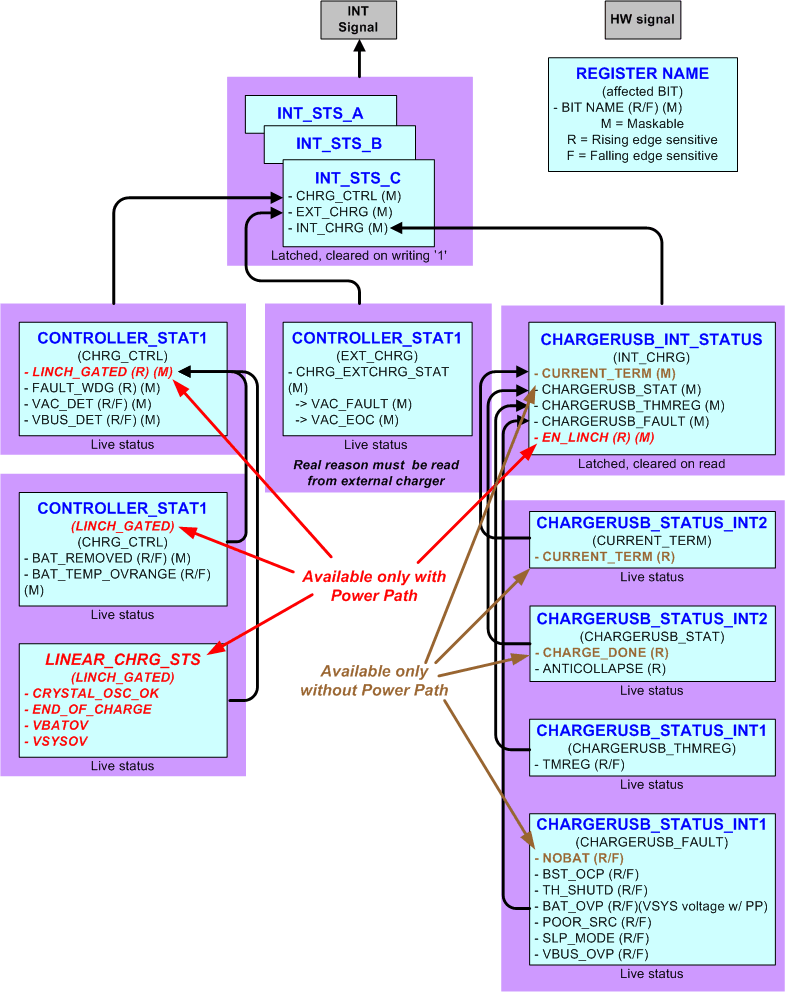 Figure 5-24 Interrupt Generation Architecture
When the INT interrupt signal is set, host processor must read the reason of the interrupt by reading the three interrupt status registers (INT_STS_A, INT_STS_B, and INT_STS_C). The battery charging related register bits (CHRG_CTRL, EXT_CHRG, and INT_CHRG) are in the INT_STS_C register. The source of the interrupt is
- CHRG_CTRL: The interrupt source is in the charger controller.
- EXT_CHRG: The interrupt source is in external charging IC.
- INT_CHRG: The interrupt source is in the TPS80032 battery charger.
The CHRG_CTRL indication can be further identified from the CONTROLLER_STAT1 register. This register shows the actual status of the different interrupt sources, so if the situation disappears before software can read it, software cannot know the real reason for the interrupt.
The origin of the external charger interrupt must be read from the external charging IC. The CHRG_EXTCHRG_STATZ bit shows the actual level of the status signal.
The source for the INT_CHRG interrupt must be further clarified in the CHARGERUSB_INT_STATUS register, which stores the latched information. The bits in the CHARGERUSB_INT_STATUS register are cleared by read access.
As an example, if the battery temperature goes above threshold level the BAT_TEMP_OVRANGE bit in CONTROLLER_STAT1 register is high. This sets LINCH_GATED bit in CONTROLLER_STAT1 register to high which sets CHRG_CTRL interrupt bit high and sets INT line low. Host processor detects the interrupt and reads INT_STS_A, INT_STS_B, INT_STS_C, CONTROLLER_STAT1 and LINEAR_CHRG_STS registers and finds the reason for the interrupt.
5.9.13.1 Sources of the Interrupt
The interrupt sources are described in the following lists, together with the actions software must take.
5.9.13.1.1 Charger Controller Interrupts
The charger controller interrupts are:
- FAULT_WDG: The charging watchdog has expired. Host processor must reset the timer in the CONTROLLER_WDG register. In addition, host must initialize the charging and restart it.
- VAC_DET: The VAC detection threshold voltage has been crossed. The VAC charger has been either inserted or removed. If the VAC charger is inserted, host processor can initialize and enable the charging and select the charging source using the CONTROLLER_CTRL1 register bits. The parameters for the VAC charging are programmed in the external IC.
- VBUS_DET: The VBUS detection threshold voltage has been crossed. The USB plug has been either inserted, removed, or the VBUS delivery has been started or stopped. If the USB plug is inserted, the host processor can initialize and enable the charging and select the charging source using the CONTROLLER_CTRL1 register bits.
- BAT_REMOVED: The battery is either removed or inserted. This battery detection is based on the pull-down resistor on the GPADC_IN0 line. This feature can be enabled and disabled using the OTP memory (EN_BAT_DET bit).
- BAT_TEMP_OVRANGE: The battery temperature has crossed the minimum or maximum temperature limit set by the external resistors. The battery charging is gated outside of the valid range automatically by hardware. This feature can be enabled and disabled using the OTP memory (EN_BAT_TEMP bit).
- CRYSTAL_OSC_OK: The charger crystal oscillator failed.
- END_OF_CHARGE: The end of charge current is detected from the linear charger loop. The host processor can terminate the charging if the battery is full. This function is valid only with Power Path (OTP bit POP_APPSCH = 1).
- VBATOV: Battery overvoltage is detected. There is something wrong in the battery charging and it should be stopped. This function is valid only with Power Path (OTP bit POP_APPSCH = 1).
- VSYSOV: System supply overvoltage is detected. There is something wrong or there is transient spike in the system supply. The system supply level must be monitored with the ADC, and if it is continuously too high, the system suppy regulator must be disabled. This function is valid only with Power Path (OTP bit POP_APPSCH = 1).
5.9.13.1.2 External Charger Interrupt
The external charger interrupt is:
- EXT_CHRG: Interrupt from the external charger IC. The reason for the interrupt must be read from the external charger IC.
5.9.13.1.3 Internal Charger Interrupts
The internal charger interrupts are:
- CURRENT_TERM: The current termination level has been detected. The functionality must be controlled by host processor using the TERM and CHARGE_ONCE bits in the CHARGERUSB_CTRL1 and CHARGERUSB_CTRL3 registers. This bit is controlled only when the PMIC is used without Power Path (OTP bit POP_APPSCH = 0).
- CHARGE_DONE: The charging termination current level is detected. Host processor can terminate the battery charging. This bit is controlled only when the PMIC is used without Power Path (OTP bit POP_APPSCH = 0).
- ANTICOLLAPSE: The anticollapse loop limiting the VBUS input voltage drop is active.
- TMREG: The thermal regulation loop of the USB charger is active. The temperature of the IC must be monitored and if it becomes too high, some power dissipation must be removed by decreasing the charging current or by disabling functions.
- NOBAT: The battery is not detected by the USB charger. This bit is controlled only when the PMIC is used without Power Path (OTP bit POP_APPSCH = 0) and the feature is enabled and disabled using the OTP bit (EN_BQBAT_DET).
- BST_OCP: The OTG boost supply overcurrent protection is active. There can be a short circuit or an excessively high load in the VBUS. The boost regulator must be disabled if the VBUS voltage is not increasing.
- TH_SHUTD: The temperature of the USB charger is higher than the threshold level and the battery charging is gated. The power dissipation must be decreased by reducing the charging current or by disabling some functions.
- BAT_OVP: The battery voltage is higher than the overvoltage threshold, and the charging is gated (without Power Path). Something may be wrong in the battery charging and it should be stopped. This bit indicates system overvoltage with Power Path.
- POOR_SRC: The VBUS voltage is between the system supply voltage and the minimum VBUS detection voltage. The voltage is too low for battery charging. The charging from VBUS must be terminated.
- SLP_MODE: The charger is in a low-power sleep mode. The VBUS voltage is below the sleep-mode entry threshold and VBUS is higher than the VBUS detection threshold.
- VBUS_OVP: The VBUS voltage is higher than the overvoltage threshold and the charging is gated. The voltage can be monitored with the ADC and if the high voltage situation continues, the charging from VBUS must be terminated by host processor.
- EN_LINCH: The linear charging has been enabled by the charger controller. This bit is controlled only when the PMIC is used with Power Path (OTP bit POP_APPSCH = 1).
WARNING
The thermal regulation loop does not work if the CIN_LIMIT[5:0] VBUS input current limit is set to unlimited. The thermal regulation loop shares the same analog loop as the VBUS input current limit and it is disabled in this situation. However, the high temperature detection still operates and it gates the DC-DC operation if triggered.
NOTE
The thermal regulation loop generates an interrupt when the DC-DC in Power Path mode and the battery charger in non-Power Path mode is enabled. The host processor must check the TMREG bit to see if the thermal regulation loop is active to identify and clear the false interrupt.
5.10 USB OTG
The device embeds all hardware analog mechanisms associated to VBUS and ID lines. The other aspects of the OTG system, such as the OTG controller (hardware/software) or the USB data line (DP/DM) with HNP and SRP signaling, are embedded in the USB PHY, which can be either integrated into the application processor or there is stand-alone USB OTG PHY.
The device supports the Battery Charging Specification Revision 1.2 and it includes hardware required for both OTG 1.3 and OTG 2.0 standards.
The device supports the following functions.
| FUNCTION/FEATURE | REGISTER/REGISTER BIT | OTG
Rev. |
MODE/STATE | SUPPLIES
NEEDED |
| SRP – Pulsing method VBUS charge on VSYS |
VBUS_CHRG_VSYS | OTG 1.3 | ACTIVE | VRTC VSYS |
| SRP – Pulsing method VBUS charge on PMID |
VBUS_CHRG_PMID | OTG 1.3 | ACTIVE | VRTC CHRG_PMID |
| SRP – Pulsing method VBUS discharge |
VBUS_DISCHRG | OTG 1.3 | ACTIVE | VRTC |
| ADP – Probing VBUS charge |
VBUS_IADP_SRC, VADP_PRB | OTG 2.0 | ACTIVE | VRTC VANA |
| ADP – Probing VBUS discharge |
VBUS_IADP_SINK, VADP_PRB | OTG 2.0 | ACTIVE | VRTC |
| ADP – Sensing | VADP_SNS | OTG 2.0 | SLEEP ACTIVE |
VRTC |
| VBUS detection | VA_VBUS_VLD, VA_SESS_VLD, VB_SESS_VLD, VB_SESS_END, VOTG_SESS_VLD | OTG 1.3 OTG 2.0 |
SLEEP ACTIVE |
VRTC VANA |
| VBUS wake-up detection | Always enabled if VBUS or VAC is present | – | PRECHARGE/OFF SLEEP/ACTIVE |
VRTC |
| VBUS GPADC measurement | VBUS_MEAS | – | ACTIVE | VRTC VANA |
| ID 220-kΩ pullup on LDOUSB | ID_PU_220K | – | ACTIVE | VRTC LDOUSB |
| ID 100-kΩ pullup on LDOUSB | ID_PU_100K | – | ACTIVE | VRTC LDOUSB |
| ID ground drive | ID_GND_DRV | – | ACTIVE | VRTC |
| ID 16-µA source current | ID_SRC_16U | BC 1.2 | PRECHARGE SLEEP/ACTIVE |
VRTC LDOUSB |
| ID 5-µA source current | ID_SRC_5U | – | ACTIVE | VRTC LDOUSB |
| ID detection | ID_GND, ID_A, ID_B, ID_C, ID_FLOAT | BC 1.2 OTG 1.3 OTG 2.0 |
PRECHARGE SLEEP/ACTIVE |
VRTC LDOUSB |
| ID wake-up detection | ID_WK_UP_COMP | – | OFF SLEEP/ACTIVE |
VRTC |
| ID GPADC measurement | ID_MEAS | – | ACTIVE | VRTC VANA |
NOTE
- Both VBUS and ID wake-up comparators can generate a start event when the device is in WAIT-ON state. The VBUS wake-up is enabled always, the ID wake-up enable is configurable and disabled by default (ID_WK_UP_COMP bit in BACKUP_REG register). Those comparators can also make the device leave the SLEEP state and enter the ACTIVE state. An interrupt is sent to the host processor if they are not masked.
- In PRECHARGE state, the VBUS wake-up comparator, the LDOUSB regulator, the ID comparators, and the 16-µA current source are enabled automatically. The ACA detection result increases the VBUS input current limit in case USB Charging Port is detected.
- The OTG_REV bit (in BACKUP_REG register) unlocks the respective VBUS detection features and associated electrical parameters specific to each OTG revision 1.3 and revision 2.0 (see the VBUS_ACT_COMP bit).
- All TPS80032 OTG registers are unlocked and operate either with a read/write (R/W) access or a read/set/clear (R/S/C) process.
- VBUS_ACT_COMP (USB_VBUS_CTRL_SET/USB_VBUS_CTRL_CLR) is the only R/W register bit that relies on the OTG_REV OTP bit value. This bit enables the needed VBUS comparators, reducing the power consumption of the OTG VBUS analog section. Therefore, all deactivated comparators have their corresponding source and latch registers fixed at 0.
- For some of the analog electrical parameters that are not backward-compatible between OTG revision 1.3 and OTG revision 2.0 but also are not manageable through the OTG_REV preselection bit, it is assumed throughout this section that the OTG revision 2.0 characteristic limits supersede the OTG revision 1.3 electrical limits and, thus, OTG 2.0 is the reference.
- OTG revision 1.3 devices have just emerged on the electronic market and should be outnumbered shortly by OTG revision 2.0 devices.
- In addition, the USB-IF consortium suggests a fast-forward transition to OTG revision 2.0 to solve current incompatibilities and limitations between OTG revision 1.3 devices.
- All electrical parametric deviations from OTG revision 1.3 are explicitly highlighted through this section.
- The full list of nonbackward-compatible electrical parameters is available on the USB-IF website in the developer forum section.
There are two types of VBUS and ID comparators, referred to throughout this section as wake-up (normally used in TPS80032 SLEEP state) and active comparators (generally activated in TPS80032 ACTIVE state). Those comparators are not exclusively working in respective TPS80032 SLEEP, and ACTIVE states, but can also pretend to additional usages’ conditions. Indeed, the wake-up comparators are targeting low power consumptions, whereas the active comparators are intended for accurate level detections:
- The wake-up comparators are working in TPS80032 PRECHARGE, WAIT-ON, SLEEP, and ACTIVE states. Those comparators can wake up the device from SLEEP state but can also switch on the device from WAIT-ON state. VBUS wake-up comparator can also start the precharge, provided that all other precharging conditions are met.
- The active comparators work in TPS80032 SLEEP and ACTIVE states. When working in the SLEEP state, all required power and clock resources should remain active. ID active comparators, used for ACA detections, are automatically enabled in PRECHARGE state; VBUS active comparators remain off.
5.10.1 ID Line
The USB Battery Charging Specification describes the operation of the ACA. The RID_A, RID_B, and RID_C resistors are related only to the different ACA operations, whereas the grounded and floating IDs (ROTG_A, ROTG_B = RID_FLOAT) are related to the connections of the USB OTG standard plugs (See "Battery Charging Specification, Revision 1.2"). When either of the RID_A, RID_B, or RID_C resistance is in place, the VBUS is delivered by the ACA. This allows the device to wake up from VBUS or ID. The host can then enable the ID active comparators by writing ID_ACT_COMP bit (in USB_ID_CTRL_SET register) to correctly identify the different RID values. In addition, an interrupt is generated if the resistance on the ID ball is changing.
During hardware-controlled charging, the TPS80032 device monitors if an ACA is connected and sets the corresponding VBUS input current limit.
The following pullup and pulldown resistors and current sources can be connected to the ID line:
- ID_PU_220K bit enables an ID 220-kΩ pullup to the LDOUSB supply.
- ID_PU_100K bit enables an ID 100-kΩ pullup to the LDOUSB supply.
- ID_GND_DRV bit enables an ID 10-kΩ pulldown.
- ID_SRC_16U bit enables an ID 16-µA current source on the LDOUSB supply.
- ID_SRC_5U bit enables an ID 5-µA current source on the LDOUSB supply.
- ID_WK_UP_COMP enables an ID 9-µA current source (IID_WK_SRC) on the VRTC supply.
The ID wake-up comparator is used when the TPS80032 device is in the WAIT-ON or SLEEP state. It allows start up of the TPS80032 device when a USB cable A-plug is attached (A-plug has a pulldown resistor, ROTG_A, to ground on the ID line).
Four comparators, supplied on the LDOUSB regulator, are implemented to evaluate the proper external ID resistor. Additional logic between those comparators allows the detection of the five debounced interrupts (fixed 30-ms debouncing):
- ID_FLOAT
- ID_A
- ID_B
- ID_C
- ID_GND
It is possible to use the GPADC to monitor the voltage on the ID line (channel 14). A 6.875-V maximum voltage on the ID line corresponds to a 1.25-V maximum dynamic at the input stage of the GPADC converter, allowing a 6.0-V maximum measurement.
Figure 5-25 shows the block diagram of the ID resistance detection and the decoding.Table 5-1 lists the ID resistance interrupt decoding.
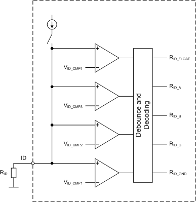 Figure 5-25 ID Resistance Detection
Table 5-1 ID Resistance Interrupt Decoding
| ID pin level | RID Resistance | Interrupt |
|---|---|---|
| VID < VID_CMP1 | RID < 1 kΩ | ID_GND |
| VID_CMP1 < VID < VID_CMP2 | 36 kΩ < RID < 37 kΩ | ID_C |
| VID_CMP2 < VID < VID_CMP3 | 67 kΩ < RID < 69 kΩ | ID_B |
| VID_CMP3 < VID < VID_CMP4 | 122 kΩ < RID < 126 kΩ | ID_A |
| VID > VID_CMP4 | RID > 220 kΩ | ID_FLOAT |
5.10.2 VBUS Line
The VBUS wake-up comparator is used when the TPS80032 device is in the PRECHARGE, WAIT-ON, SLEEP, or ACTIVE state. It allows startup of the TPS80032 device when a USB cable plug is attached with a VBUS voltage level of 3.6 V minimum being present on the VBUS line.
The LDOUSB regulator, the ACA comparators and 16-µA current source can be selected to be controlled by the VBUS wake-up comparator until the first I2C write access to the LDOUSB resource state register (LDOUSB_CFG_STATE) (by setting the AUTO_LDOUSB_DIS OTP bit to 0).
The following pullup and pulldown resistors and current sinks/sources can be connected to the VBUS line:
- VBUS_CHRG_VBAT bit enables a VBUS 2-kΩ pullup to the VSYS supply.
- VBUS_CHRG_PMID bit enables a VBUS 2-kΩ pullup to the CHRG_PMID supply.
- VBUS_DISCHRG bit enables a VBUS 10-kΩ pulldown.
- VBUS_IADP_SRC bit enables a VBUS 1.4-mA current source on the VANA supply.
- VBUS_IADP_SINK bit enables a VBUS 1.5-mA current sink.
- RA_BUS_IN resistor is fixed and a combination of all parallel resistor bridges implemented on VBUS in the various IPs such as backup battery, OTG, and charger.
- RVBUS_LKG represents the TPS80032 device internal leakage.
Related to the OTG 1.3 revision, four comparators supplied on the VANA regulator are implemented to evaluate the proper voltage level on the VBUS line.
In the OTG 2.0 revision, only one comparator is required for the session valid detection (VOTG_SESS_VLD) supplied also on the VANA domain. Still, the VA_VBUS_VLD comparator can be used to detect a possible VBUS short-circuit condition.
The TPS80032 device embeds the OTG 2.0 optional features related to the VBUS ADP probing and sensing, and hence with two additional comparators supplied on VANA (VADP_PRB and VADP_SNS).
Seven comparators allow the detection of the four OTG 1.3 and the three OTG 2.0 debounced interrupts:
- VA_VBUS_VLD (OTG 1.3/OTG 2.0) – fixed 30-ms debouncing
- VB_SESS_VLD (OTG 1.3) – fixed 30-ms debouncing
- VA_SESS_VLD (OTG 1.3) – fixed 30-ms debouncing
- VB_SESS_END (OTG 1.3) – fixed 30-ms debouncing
- VOTG_SESS_VLD (OTG 2.0) – fixed 30-ms debouncing
- VADP_PRB (OTG 2.0) – fixed 2x 30-µs debouncing
- VADP_SNS (OTG 2.0) – fixed 2x 30-µs debouncing
It is possible to use the GPADC to monitor the voltage on the VBUS line (channel 10), see GENERAL-PURPOSE ADC for more information.
NOTE
- If the system switches off, the LDOUSB regulator stays on if the VBUS is still connected.
- When the NRESPWRON signal is released, only I2C accesses enable the regulator, if not previously enabled by the VBUS wake-up comparator in the PRECHARGE state.
- The LDOUSB regulator is a dual-input supply LDO. The LDOUSB regulator enable is independent of the overvoltage condition.
- When a VBUS overvoltage condition occurs, the CHRG_PMID input switch is automatically opened, protecting the LDOUSB from possible overvoltage stresses.
- When neither the VSYS nor PMID input supply is selected, the LDOUSB regulator cannot output a proper voltage, even if its control enable is set (see the LDOUSB_CFG_TRANS register).
- Host should keep monitoring the VBUS overvoltage condition and turn off the LDOUSB regulator when necessary.
- The VBUS detection mechanism works only when the VANA supply is present:
- TPS80032 SLEEP state – VANA should remain active.
- TPS80032 ACTIVE state – VANA is always on.
- For ADP detection, host can use the TPS80032 embedded mechanism or directly use the output of the comparators with their associated interrupts.
- There is no source and enable low register bits associated with the ADP interrupt, because this ADP interrupt represents the output of the digital ADP module and not the output of an analog comparator.
5.10.3 ADP on VBUS Line
The ADP lets the device detect when a remote device is attached or detached with a low power consumption. The ADP detects the change in the VBUS capacitance that occurs when two devices are attached or detached. The capacitance is detected by first discharging (VBUS_IADP_SINK) the VBUS line and then measuring the time it takes for VBUS to charge to a VADP_PRB voltage level with a VBUS_IADP_SRC current source. The change in the capacitance is detected by looking for a change in the T_ADP_RISE charge time. This procedure is called ADP probing.
If an A-device is attached to a B-device, and both support ADP features, the A-device performs ADP probing and the B-device performs ADP sensing. During ADP sensing, the B-device looks for ADP probing activity on the VBUS line. If ADP probing activity is detected, the B-device determines that the A-device is still attached.
As shown in Figure 5-26, the ADP module has timing register bits (T_ADP_HIGH, T_ADP_LOW, and T_ADP_RISE), control logic, a current source (VBUS_IADP_SRC), a current sink (VBUS_IADP_SINK), and two comparators (VADP_PRB [ADP probing] and VADP_SNS [ADP sensing]).
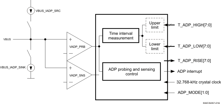 Figure 5-26 Attach Detection Protocol Scheme
Figure 5-27 shows the ADP timing diagram.
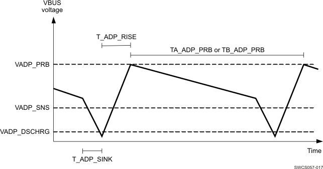 Figure 5-27 ADP Timing Diagram
| ADP_MODE[1:0] | OPERATION |
|---|---|
| 00 | ADP digital module is disabled. |
| 01 | ADP sensing mode is enabled. |
| 10 | ADP probing mode as an A-device is enabled. |
| 11 | ADP probing mode as a B-device is enabled. |
The limit registers (T_ADP_LOW[7:0] and T_ADP_HIGH[7:0]) and the last measurement time (T_ADP_RISE[7:0]) are reset when the digital module is disabled.
During the ADP sensing mode, the VADP_SNS comparator is used. The digital module monitors the comparator output to ensure that it toggles and the time duration between the rising edge of the comparator output signal is shorter than T_ADP_SNS. If there is no new rising edge within the T_ADP_SNS period, the module generates an ADP interrupt.
Figure 5-28 shows the ADP sensing timing diagram.
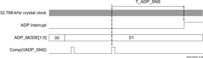 Figure 5-28 ADP Sensing Timing Diagram
During ADP probing, the VADP_PRB comparator is used. The time interval measurement counter is reset and the VBUS_IADP_SINK current sink is turned on for T_ADP_SINK. The T_ADP_SINK time is long enough to discharge the VBUS voltage below VADP_DSCHG. There is no comparator to monitor the discharge level. After that, the current sink is turned off, the current source VBUS_IADP_SRC is turned on, and the time interval measurement counter starts to count 32.768-kHz crystal clock cycles. When the VBUS voltage reaches VADP_PRB voltage level the current source is turned off, and the time interval measurement counter is stopped. If the VADP_PRB voltage is not reached before counter value is 255, the counter value is stopped to 255. The current source is disabled when the voltage reaches VADP_PRB level or the next current sink period starts. If the measured time interval value is lower than T_ADP_LOW[7:0] or higher than T_ADP_HIGH[7:0], an interrupt is generated. The host processor sets the limit values so that the operation fulfills the requirements of the OTG 2.0 specification. Figure 5-29 shows the ADP probing timing diagram.
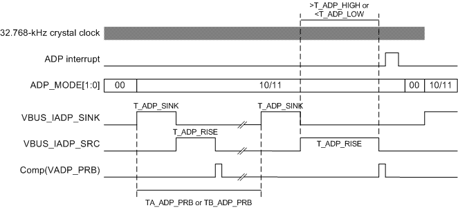 Figure 5-29 ADP Probing Timing Diagram
5.11 Gas Gauge
The gas gauge, also called the current gauge, measures the current from the battery or the current into the battery. An ADC (Coulomb counter) is required to measure the voltage over the external sense resistor, R2. This resistor is connected to the negative side of the battery. The integration period of the ADC is programmable from 3.9 to 250 ms with CC_ACTIVE_MODE[1:0] bits (in FG_REG_00 register). The gas gauge works continuously, which means that the new measurement starts immediately after the previous result becomes available. The accumulated result is calculated by the TPS80032 digital module but requires host processor to calculate the battery energy (See ).
Figure 5-30 shows a block diagram of the gas gauge.
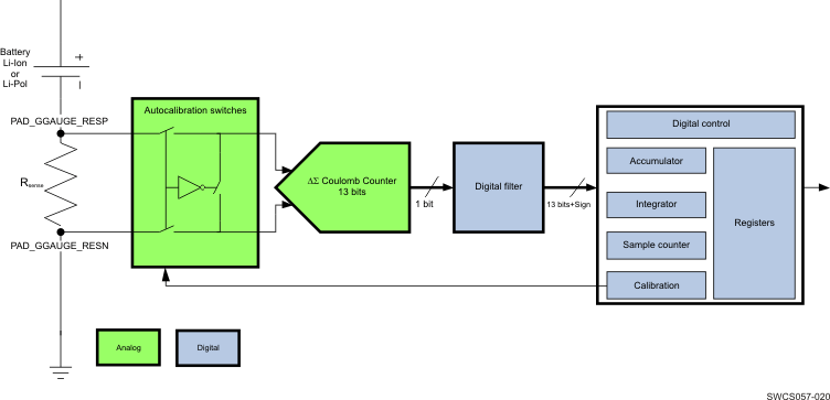 Figure 5-30 Gas Gauge Block Diagram
5.11.1 Autocalibration
Autocalibration is enabled by host. During autocalibration, the gas gauge performs eight measurements so that the inputs for the ADC are short-circuited. The result indicates the offset error of the gas gauge. The result is stored in the CC_OFFSET[9:0] bits and the completion of the measurement procedure is indicated with the CC_AUTOCAL interrupt. Software must read the offset error result (CC_OFFSET[9:0] bits in FG_REG_08 and FG_REG_09 registers) and use that to compensate the actual measurement results. The CC_CAL_EN bit self-clears when the calibration completes. The gas gauge must be enabled (FGS bit TOGGLE1 register) before starting the calibration. The temperature variation changes the offset error, so the recalibration is preferred during operation.
5.11.2 Auto-Clear and Pause
The auto-clear function is used in the sequence of changing from one integration period to another. Before changing the integration period, the CC_PAUSE bit must be set to 1. Setting the CC_AUTOCLEAR bit to 1 clears the CC_OFFSET[9:0], CC_SAMPLE_CNTR[23:0], and CC_ACCUM[31:0] bit fields. The CC_AUTOCLEAR bit self-clears when the registers are reset.
Setting CC_PAUSE to 1 keeps the analog from updating the integrator, accumulator, and sample counter registers. The integrator continues to run. If an integration period ends while the CC_PAUSE bit is 1, the value that is normally written to these registers is lost and the next integration period starts automatically.
5.11.3 Dithering
The FGDITHS bit is set to 1 to enable dithering in the ADC, which keeps idle tones from being generated with a DC input value. FGDITHS is not affected by the CC_AUTOCLEAR bit. Use the FGDITHR bit to disable the dithering. The dithering feature status is available in the FGDITH_EN bit.
5.11.4 Operation Guidelines
In order to start the current gauging the host processor must first set the correct integration period (CC_ACTIVE_MODE[1:0] bits), enable the gas gauge (FGS toggle bit), and perform the calibration (CC_CAL_EN bit) to get the offset error and use that to make corrections to the measurement results. The current gauge enters normal operation automatically when calibration completes. After that, host processor can read the sample counter (CC_SAMPLE_CNTR[23:0] bits) and accumulator (CC_ACCUM[31:0] bits) results and calculate the energy accordingly.
To record the current consumption waveform,the host must use an interrupt (CC_EOC) to detect when the integration sample result is ready. The integration register CC_INTEG[13:0] always stores the result of the last measurement.
WARNING
Anti-aliasing filter (RC-filtering) is not allowed with Charger Power Path configuration. The charger senses the battery current using the same resistor as Gas Gauge and RC filtering affects the charger loops and may generate stability problems.
5.12 General-Purpose ADC
The GPADC consists of a 12-bit sigma-delta ADC combined with a 19-input analog multiplexer. The GPADC enables the host processor to monitor a variety of analog signals using analog-to-digital conversion on the input source. After the conversion completes, an interrupt is generated (GPADC_RT_EOC or GPADC_SW_EOC) for the host processor and it can read the result of the conversion through the I2C interface.
The GPADC supports 19 analog inputs: 7 of these inputs are available on external balls and the remaining 12 are dedicated to internal resource monitoring. Two of the seven external inputs are associated with current sources allowing measurements of resistive elements (battery type and temperature or other thermal sensor). The reference voltage (GPADC_VREF) is available when the GPADC is enabled.
GPADC_IN0 is associated with a current source of 7 µA. An additional 15-µA current source can be enabled by register bit (GPADC_ISOURCE_EN bit in GPADC_CTRL register). A comparator connected to this input is intended to detect the presence or absence of the battery (resistance to ground is less than 130 kΩ in the battery pack). The removal and insertion of the battery pack generates an interrupt and the detection result is also available at the BATREMOVAL ball.
GPADC_IN1 and GPADC_IN4 are associated with a voltage reference equal to the ADC reference and are intended to measure temperature with an NTC sensor. In addition, a detection module is connected to GPADC_IN1 to permanently monitor the temperature and gate the charge for the battery.
GPADC_IN3 is associated with the three selectable current sources and can be used, for example, to measure a voltage across an external resistor or diode. The selectable current levels are 10 µA, 400 µA, and 800 µA and the current is controlled by a register bits (GPADC_REMSENSE[1:0] bits in GPADC_CTRL2 register).
Figure 5-31 shows the block diagram of the GPADC.
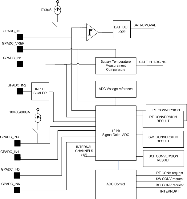 Figure 5-31 Block Diagram of the GPADC
For all the measurements performed by the monitoring ADC, the means to scale of the signal to be measured to the ADC input range are integrated in the TPS80032 device (voltage dividers, current to voltage converters, and current source).
The conversion requests are initiated by the host processor, either by software through the I2C or by hardware through a dedicated external ball GPADC_START. This last mode is useful when real-time conversion is required. An interrupt signal is generated when the conversion result is ready.
There are three kinds of conversion requests with the following priority:
- Real-time conversion request (RT)
- Asynchronous conversion request (SW)
- Battery charging module internal conversion request (BCM)
Before starting the measurement, the software can enable channels, scalers, current sources and select other parameters:
- GPADC_IN0: Additional current source with the GPADC_ISOURCE_EN bit in the GPADC_CTRL register. (Can be enabled only if OTP bit EN_BAT_DET=1)
- GPADC_IN1: Enable channel with the GPADC_TEMP1_EN bit in the GPADC_CTRL register.
- GPADC_IN2: Enable channel with the GPADC_SCALER_EN_CH2 bit in the GPADC_CTRL register.
- GPADC_IN3: Select current source level with the GPADC_REMSENSE [1:0] bits in the GPADC_CTRL2 register.
- GPADC_IN4: Enable channel with the GPADC_TEMP2_EN bit in GPADC_CTRL the register.
- GPADC_IN7: Select scaler ratio with the VSYS_SCALER_DIV4 bit in GPADC_CTRL the register.
- GPADC_IN11: Enable channel with the GPADC_SCALER_EN_CH11 bit in GPADC_CTRL the register.
- GPADC_IN12: Enable channel with the TMP1_EN_MONITOR bit in GPADC_CTRL the register.
- GPADC_IN13: Enable channel with the TMP2_EN_MONITOR bit in GPADC_CTRL the register.
- GPADC_IN18: Enable channel with the GPADC_SCALER_EN_CH18 bit and select scaler ration with the VBAT_SCALER_DIV4 bit in the GPADC_CTRL2 register.
- Polarity of the GPADC_START signal for RT measurement: GPADC_START_POLARITY bit in the TOGGLE1 register.
- Sampling window time (16.5 μs / 450 μs): GPADC_SAMP_WINDOW bit in the TOGGLE1 register.
5.12.1 Real-Time Conversion Request (RT)
The real-time conversion is requested with the GPADC_START signal. Before requesting the conversion, software must enable the required channels, scalers, and current sources. In addition, software must enable the GPADC with the GPADCS bit in the TOGGLE1 register and select one or two channels for conversion with the RTSELECT_LSB, RTSELECT_ISB, and RTSELECT_MSB register bits. If more than two channels are selected for the conversion, the two lowest input numbers are converted. At the end of the conversions, the GPADC writes the conversion results into the results register (RTCH0_LSB, RTCH0_MSB, RTCH1_LSB, and RTCH1_MSB) and sets the GPADC_RT_EOC interrupt (if interrupt is unmasked).
If a GPADC_START real-time request occurs while a software-initiated conversion or BCM internal conversion is running, the ongoing conversion is aborted, the real-time conversion is started, and a new software-initiated or BCM internal conversion is rescheduled after the real-time conversion is ready.
5.12.2 Asynchronous Conversion Request (SW)
Software can also request a conversion asynchronously with respect to the GPADC_START signal. This conversion is not critical in terms of start-of-conversion positioning.
Software enables the required channels, scalers, current sources, enables the GPADC with GPADCS bit in TOGGLE1 register and selects the channel to be converted with GPSELECT_ISB register bits. The conversion is requested with SP1 bit in the CTRL_P1 register. When the conversion is ready a GPADC_SW_EOC interrupt is generated (if interrupt is unmasked) and the conversion result is available in GPCH0_LSB and GPCH0_MSB registers. A GPADC_START-initiated conversion (RT) and BCM internal conversion have higher priority than the software-initiated conversion.
If a software request occurs while a GPADC_START-initiated sequence (RT) or BCM internal conversion is running, the software request is placed on hold and the ongoing conversion continues until it completes and the converted data is stored. A GPADC_RT_EOC interrupt is then generated and sent to the processor in case of RT sequence. The digital control executes the software request when the higher priority conversion are completed. A GPADC_SW_EOC interrupt is then generated.
5.12.3 BCM Internal Conversion Request
The GPADC is automatically enabled when an internal BCM request is asserted. When this occurs, the GPADC input channel 17 is selected for a conversion. At the end of the conversion, the GPADC result is passed internally to the BCM digital control. Interrupt is not generated at the end of the BCM conversion request.
GPADC_START-initiated conversion (RT) has a higher priority than the BCM-initiated conversion.
The different ADC channels are summarized in the following table.
Table 5-2 GPADC Input Channels
| CHANNEL | TYPE | INPUT VOLTAGE FULL RANGE(1) | INPUT VOLTAGE PERFORMANCE RANGE(2) | OPERATION |
|---|---|---|---|---|
| 0 | External | 0–1.25 V(3) | 0.01–1.215 V | Battery type, resistor value |
| 1 | External | 0–1.25 V(3) | 0.01–1.215 V | Battery temperature, NTC resistor value |
| 2 | External | 0–1.875 V(3) | 0.015–1.822 V | Audio accessory/general purpose |
| 3 | External | 0–1.25 V(3) | 0.01–1.215 V | Temperature with external diode/general purpose |
| 4 | External | 0–1.25 V(3) | 0.01–1.215 V | Temperature measurement/general purpose |
| 5 | External | 0–1.25 V(3) | 0.01–1.215 V | General purpose |
| 6 | External | 0–1.25 V(3) | 0.01–1.215 V | General purpose |
| 7 | Internal | 0–5 V or 0–6.25 V | 0.04–4.86 V or 0.05–6.075 V | System supply |
| 8 | Internal | 0–6.25 V | 0.05–4.8 V | Backup battery |
| 9 | Internal | 0–11.25 V | 2.0–10.0 V | External charger input |
| 10 | Internal | 0–27.25 V | 0.01–6.0 V | VBUS |
| 11 | Internal | 0–1.875 A | 0.015–1.5 A | VBUS DC-DC output current (available only without power path, OTP memory bit POP_APPSCH = 0, R9 = 68 mΩ) |
| 12 | Internal | 0–1.25 V | 0.01–1.215 V | Die temperature |
| 13 | Internal | 0–1.25 V | 0.01–1.215 V | Die temperature |
| 14 | Internal | 0–6.875 V | 0.055–6.68 V | USB ID line |
| 15 | Internal | 0–6.25 V | 0.05–6.075 V | Test network |
| 16 | Internal | 0–4.75 V | 0.038–4.617 V | Test network |
| 17 | Internal | 0–7.8125 A | 0–1.5 A | Battery charging current (with 20-mΩ sense resistor) (available only with power path, OTP memory bit POP_APPSCH = 1) |
| 18 | Internal | 0–5 V or 0–6.25 V | 0.04–4.86 V or 0.05–6.075 V | Battery voltage |
5.12.4 Calibration
The GPADC channels are calibrated in the production line using a two point calibration method. The channels are measured with two known values (X1 and X2) and the difference (D1 and D2) to the ideal values (Y1 and Y2) are stored in OTP memory. The principle of the calibration is shown in Figure 5-32.
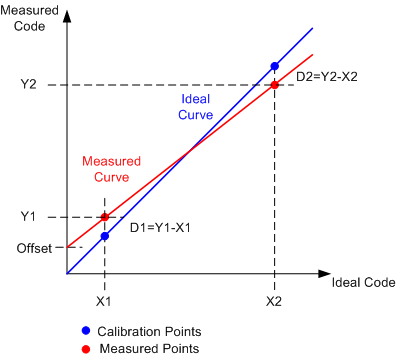 Figure 5-32 ADC Calibration Scheme
The corrected result can be calculated using the following equations.
Gain: k = 1 + ((D2 – D1) / (X2 – X1))
Offset: b = D1 – (k - 1) × X1
If the measured code is a, the corrected code a' is:
a' = (a – b) / k
Some of the GPADC channels can use the same calibration data. Table 5-3 lists the parameters X1 and X2, and the register of D1 and D2 needed in the calculation for all the channels.
Table 5-3 GPADC Calibration Parameters
| CHANNEL | X1 | X2 | D1(1) | D2(1) | COMMENTS |
|---|---|---|---|---|---|
| 0, 1, 3, 4, 5, 6, 12, 13 | 1441 (0.44 V) |
3276 (1.0 V) |
GPADC_TRIM3[4:0] * 4 + GPADC_TRIM1[2:1], sign = GPADC_TRIM1[0] | GPADC_TRIM4[5:0] * 4 + GPADC_TRIM2[2:1], sign = GPADC_TRIM2[0] | Channel 3 trimming is used |
| 2 | 1441 (0.66 V) |
3276 (1.5 V) |
GPADC_TRIM3[4:0] * 4 + GPADC_TRIM1[2:1], sign = GPADC_TRIM1[0] | GPADC_TRIM4[5:0] * 4 + GPADC_TRIM2[2:1], sign = GPADC_TRIM2[0] | Channel 3 trimming is used |
| 8 | 1441 (2.2 V) |
3276 (5.0 V) |
(GPADC_TRIM3[4:0] * 4 + GPADC_TRIM1[2:1], sign = GPADC_TRIM1[0]) + (GPADC_TRIM8[4:3] * 16 + GPADC_TRIM7[4:1], sign = GPADC_TRIM7[0]) | (GPADC_TRIM4[5:0] * 4 + GPADC_TRIM2[2:1], sign = GPADC_TRIM2[0]) + (GPADC_TRIM10[4:0] * 4 + GPADC_TRIM8[2:1], sign = GPADC_TRIM8[0]) | Channel 3 and channel 8 trimming is combined |
| 9 | 1441 (3.96 V) |
3276 (9.0 V) |
(GPADC_TRIM3[4:0] * 4 + GPADC_TRIM1[2:1], sign = GPADC_TRIM1[0]) + (GPADC_TRIM14[4:3] * 16 + GPADC_TRIM12[4:1], sign = GPADC_TRIM12[0]) | (GPADC_TRIM4[5:0] * 4 + GPADC_TRIM2[2:1], sign = GPADC_TRIM2[0]) + (GPADC_TRIM16[4:0] * 4 + GPADC_TRIM14[2:1], sign = GPADC_TRIM14[0]) | Channel 3 and channel 9 trimming is combined |
| 10 | 150 (1.0 V) |
751 (5.0 V) |
GPADC_TRIM11[3:0] * 8 + GPADC_TRIM9[3:1], sign = GPADC_TRIM9[0] | GPADC_TRIM15[3:0] * 8 + GPADC_TRIM13[3:1], sign = GPADC_TRIM13[0] | Dedicated trimming |
| 11 | 1441 (0.66 A) |
3276 (1.5 A) |
GPADC_TRIM3[4:0] * 4 + GPADC_TRIM1[2:1], sign = GPADC_TRIM1[0] | GPADC_TRIM4[5:0] * 4 + GPADC_TRIM2[2:1], sign = GPADC_TRIM2[0] | Channel 3 trimming is used |
| 14 | 1441 (2.42 V) |
3276 (5.5 V) |
GPADC_TRIM3[4:0] * 4 + GPADC_TRIM1[2:1], sign = GPADC_TRIM1[0] | GPADC_TRIM4[5:0] * 4 + GPADC_TRIM2[2:1], sign = GPADC_TRIM2[0] | Channel 3 trimming is used |
| 7, 18 | 1441 (2.2 V) |
3276 (5.0 V) |
(GPADC_TRIM3[4:0] * 4 + GPADC_TRIM1[2:1], sign = GPADC_TRIM1[0]) + (GPADC_TRIM5[6:1], sign = GPADC_TRIM5[0]) | (GPADC_TRIM4[5:0] * 4 + GPADC_TRIM2[2:1], sign = GPADC_TRIM2[0]) + (GPADC_TRIM6[7:1], sign = GPADC_TRIM6[0]) | Channel 3 and channel 18 trimming is combined, input voltage range is 0–6.25 V |
| 17 | Icharge = (a – GPADC_TRIM20[7:0]) * (1 + GPADC_TRIM21[5:0] / 512) * 1.25 V / 4096 / 8 / R2 ; a = measured code, GPADC_TRIM20[7:0] is an unsigned value, in GPADC_TRIM21[5:0] the bit 5 is the sign and bits[4:0] are the magnitude |
Dedicated equation | |||
5.13 Vibrator Driver and PWM Signals
The LDO3 regulator can be used as a generic voltage supply or as a vibrator motor driver. The output voltage level is controlled with the LDO3_CFG_VOLTAGE register and the regulator provides output current up to 200 mA.
The vibrator mode is selected with the SEL_VIB bit in the MISC2 register. The duty cycle and frequency are controlled with the DSEL[1:0] and FREQ[1:0] bits in the VIBCTRL and VIBMODE registers. The vobrator is started with the VIBS bit and stopped with the VIBC bit in the TOGGLE2 register. The vibrator driver allows a soft turn on (500-µs maximum) and turn off (2-ms maximum).
Figure 5-33 shows a block diagram of the vibrator motor driver.
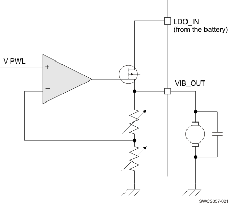 Figure 5-33 Block Diagram of Vibrator Motor Driver
The PWM1 and PWM2 digital outputs provide PWM signals on the 1.8-V I/O domain. The current drive capability of both PWM buffer is 4 mA and the outputs can also be active when the system is in the SLEEP state.
The period of the PWM signals can be selected separately with the PWM1_LENGTH and PWM2_LENGTH bits in the PWM1ON and PWM2ON registers. The selection of 128 clock cycles results as a 256-Hz PWM signal and the selection of 64 cycles results as 512-Hz PWM signal. Both PWM signals have dedicated counters. The counters are started by first enabling the 32768-Hz clock inputs with the PWM1EN and PWM2EN bits in the TOGGLE3 register and then setting the PWM1S and PWM2S bits. The rising and falling-edge positions are selected with the PWM1ON[6:0], PWM1OFF[6:0], PWM2ON[6:0], and PWM2OFF[6:0] bits in the PWM1ON, PWM1OFF, PWM2ON, and PWM2OFF registers as shown in Figure 5-34.
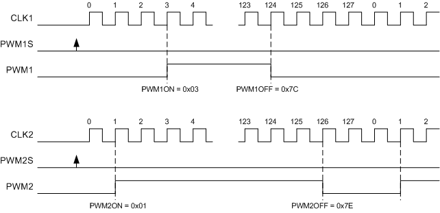 Figure 5-34 PWM Signal Timings (128 Clock Cycles in Period, Clocks Synchronized)
NOTE
The clock inputs for generation of PWM signals are enabled with the PWM1EN and PWM2EN bits in the TOGGLE3 register. The start and stop of the PWM signal generation is controlled with the PWM1S, PWM2S, PWM1C, and PWM2C bits in the TOGGLE3 register. To get a clean start and stop, the clock input must be enabled before starting PWM signal generation and the PWM signal generation must be stopped before disabling the clock input. The CLK1 and CLK2 counters can be synchronized by setting both the PWM1S and PWM2S bits high with the same I2C write.
The PWM signal is constantly high if PWMxON[6:0] is equal to PWMxOFF[6:0].
The following rules must be fulfilled for the PWMxON and PWMxOFF settings:
- PWMxOFF[6:0] ≥ PWMxON[6:0]
- PWMxON[6:0] > 0x00
5.14 Detection Features
The TPS80032 device supports the following detection functions:
- Detection of SIM card insertion and extraction with programmable debouncing using SIM pin, automatic power shutdown of LDO7 when extraction is detected (configurable)
- Detection of MMC card insertion and extraction with programmable debouncing using MMC pin, automatic power shutdown of LDO5 when extraction is detected (configurable)
- Detection of battery presence and removal with GPADC_IN0 input (see Section 5.9.8)
The TPS80032 device supports SIM card and MMC card insertion and extraction detections with programmable debounce times. The debounce times are programmed with SIMDEBOUNCING and MMCDEBOUNCING registers. When the SIM card or MMC card is inserted, a mechanical contact connected on the TPS80032 device terminal SIM or MMC is tripped, and after debouncing an interrupt is generated. The SIM card and MMC card presence detection logic is active even when the system is in idle mode; the debouncing logic (programmable) is based on the 32-kHz clock. When a card insertion is detected, the required regulator must be enabled by host processor. When a card is extracted, the LDO7 for SIM card and LDO5 for MMC card can be selected to turn off automatically. These are controlled by SIMCTRL and MMCCTRL registers. An interrupt is generated when a plug or unplug is detected.
The SIM card or MMC card plug and battery insertion/extraction are detected in SLEEP and ACTIVE states. Both card detections and battery detection have dedicated maskable interrupts (MMC, SIM, and BAT).
5.15 Thermal Monitoring
The TPS80032 device includes several different thermal monitoring functions:
- Thermal protection module in the TPS80032 device, close to SMPSs and LDOs
- Thermal shutdown for system supply regulator inside the TPS80032 device
- Battery temperature monitoring with external NTC resistor (can be used to gate the battery charging)
- Platform temperature monitoring with external NTC resistor
- Platform temperature monitoring with external diode
A thermal protection module inside the TPS80032 device monitors the temperature of the device. It generates a warning to the system when excessive power dissipation occurs and shuts down the TPS80032 device if the temperature rises to a value at which damage can occur.
CAUTION
The silicon technology used to build the TPS80032 device supports a maximum operating temperature of 150°C. Regarding packaging technology, a continuous operation above 125°C requires special packaging and must be avoided.
By default, thermal protection is always enabled except in the BACKUP or OFF state.
The TPS80032 device integrates two HD detection mechanisms to monitor and alert the host that the junction temperature is rising and must take action to reduce consumption. Those mechanisms are placed on two opposite sides of the chip and closed to the LDOs and SMPSs. Even if there are two identical thermal feature instances on the chip, it is always considered through the specification to be unique. In addition to those HD detections, there is another HD feature embedded in the system supply regulator. This HD is specified in Section 5.9, Battery Charging, and does not behave exactly as described in the following section.
5.15.1 Hot-Die Function
The HD detector monitors the temperature of the die and provides a warning to the host processor through the interrupt (HOT_DIE) when temperature reaches a critical value. The temperature threshold value is programmable with the THERM_HD_SEL[1:0] bits in the TMP_CFG register. The threshold has typically 10°C hysteresis to avoid the generation of multiple interrupts.
When an interrupt is triggered by the power-management software, immediate action to reduce the amount of power drawn from the TPS80032 device must be taken (for example, noncritical applications must be closed).
5.15.2 Thermal Shutdown
The thermal shutdown detector monitors the temperature on the die. If the junction reaches a temperature at which damage can occur, a switch-off transition is initiated and a thermal shutdown event is written into a status register.
To avoid interrupts at restart, the system cannot be restarted until the die temperature falls below the HD threshold.
The thermal shutdown monitor function is integrated to generate an immediate, unconditional TPS80032 device switch off when an overtemperature condition exists. This function must be distinguished with the early warning provided to host processor by the HD monitor function.
In the TPS80032 device, the threshold (TJ rising) of the thermal shutdown is 148°C nominal. The thermal shutdown hysteresis is 10°C in typical conditions. The reset generation is debounced. The thermal shutdown function can be masked only in the SLEEP state (the TMP_CFG_TRANS register) and in test mode.
5.15.3 Temperature Monitoring with External NTC Resistor or Diode
The GPADC_IN1 and GPADC_IN4 channels can be used to measure a temperature with an external NTC resistor. External pullup and pulldown resistors can be connected to the input to linearize the characteristics of the NTC resistor. GPADC_IN1 can be used to gate the battery charging at invalid temperatures. The temperature limits are set by external resistors.
GPADC_IN3 can be used to measure the temperature with external diode. The input channel has three selectable current sources.
5.16 I2C Interface
A general-purpose serial control interface (CTL-I2C) allows read-and-write access to the configuration registers of all resources of the system.
A second serial control interface (DVS-I2C) is dedicated to dynamic voltage scaling (DVS).
Both control interfaces comply with the HS-I2C specification and support the following features:
- Mode: Slave only (receiver and transmitter)
- Speed
- Standard mode (100 kbps)
- Fast mode (400 kbps)
- High-speed mode (3.4 Mbps)
- Addressing: 7-bit mode addressing device
The following features are not supported:
- 10-bit addressing
- General call
5.17 Secure Registers
Certain registers of the TPS80032 device can be protected by restricting their access in write mode to software running in the secure mode. Read access to protected registers is always possible. Secure access is enabled or disabled by the MSECURE control signal.
The following components or actions can be protected:
- All RTC registers
- 64 bits of general-purpose memory (8 × 8) in the VALIDITY backup domain
The read accesses are independent to the MSECURE value.
When MSECURE is logical level 1, all read and write accesses are authorized; when MSECURE is logical level 0, only read accesses are authorized.
The MSECURE detection security feature is enabled and disabled by an OTP bit.
5.18 Access Protocol
For compatibility purpose, the I2C interface of the TPS80032 device uses the same read/write protocol based on an internal register size of 8 bits as do other TI power ICs. Supported transactions are described in the following sections.
5.18.1 Single-Byte Access
A write access is initiated by a first byte including the address of the device (7 most-significat bits [MSBs]) and a write command (least-significant bit [LSB]), a second byte provided the address (8 bits) of the internal register, and the third byte represents the data to be written in the internal register.
Figure 5-35 shows a write access single-byte timing diagram.
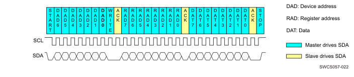 Figure 5-35 I2C Write Access Single Byte
A read access is initiated by:
- A first byte, including the address of the device (7 MSBs) and a write command (LSB)
- A second byte, providing the address (8 bits) of the internal register
- A third byte, including again the device address (7 MSBs) and the read command (LSB)
The device replies by sending a fourth byte representing the content of the internal register.
Figure 5-36 shows a read access single-byte timing diagram.
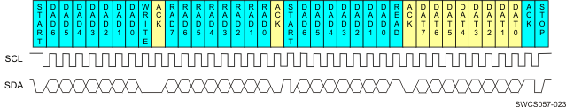 Figure 5-36 I2C Read Access Single Byte
5.18.2 Multiple-Byte Access to Several Adjacent Registers
A write access is initiated by:
- A first byte, including the address of the device (7 MSBs) and a write command (LSB)
- A second byte, providing the base address (8 bits) of the internal registers
The following N bytes represent the data to be written in the internal register, starting at the base address and incremented by 1 at each data byte.
Figure 5-37 shows a write access multiple-byte timing diagram.
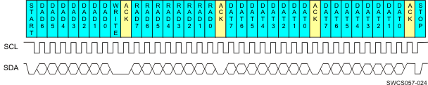 Figure 5-37 I2C Write Access Multiple Bytes
A read access is initiated by:
- A first byte, including the address of the device (7 MSBs) and a write command (LSB)
- A second byte, providing the base address (8 bits) of the internal register
- A third byte, including again the device address (7 MSBs) and the read command (LSB)
The device replies by sending a fourth byte representing the content of the internal registers, starting at the base address and next consecutive ones.
Figure 5-38 shows a read acces multiple-byte timing diagram.
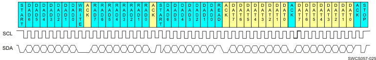 Figure 5-38 I2C Read Access Multiple Bytes
5.19 Interrupts
The INT signal (active low) indicates the host processor of events occurring on the TPS80032 device. The host processor then reads the interrupt status registers (INT_STS_A, INT_STS_B, and INT_STS_C) through I2C to identify the interrupt source. Each interrupt source can be individually masked through the interrupt mask registers. If the source is masked with mask line register (INT_MSK_LINE_A, B, C) then the INT signal is not generated for host processor but the interrupt status register (INT_STS_A, B, C) is set in case of source event. If the source is masked with mask status register (INT_MSK_STS_A, B, C) then the INT signal is not generated and the status register is not set in case of source event. The block diagram of the interrupt handler is shown in Figure 5-39.
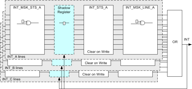 Figure 5-39 Block Diagram of Interrupt Handler
In order to clear the status registers and the interrupt signal, a write in any of the status registers (INT_STS_A, B, or C) must be done. Each write has the same effect (interrupt line goes high and all status registers are cleared). This requires that the three status registers must be read before acknowledging the interrupt to avoid losing any interrupt sources.
If additional interrupt or interrupts occur while the status registers and interrupt line are not cleared, the status registers are not updated immediately. Instead, the interrupts are held pending in a shadow registers. When the previous interrupt(s) are cleared, the interrupt line goes high and the content of the shadow registers is moved to status registers. If there are new unmasked events the interrupt signal is set to low again.
If the unmasked source event occurs when the INT signal is high, the interrupt status bit is set without using the shadow register.
NOTE
- An interrupt associated with a function must be masked before enabling or disabling the feature; otherwise, it might generate a false interrupt directly linked to the state change of the source and not related to a detection event (for example, a SYS_VLOW interrupt with the VSYSMIN_HI comparator).
- INT is always active low.
- When a interrupt occurs:
- Software should first read all status registers INT_STS_A, INT_STS_B, and INT_STS_C.
- Execute the subroutines related to the read interrupts.
- Clear the interrupt signal and interrupt status of all status registers.
| # | REG | BIT | SECTION | INTERRUPT | Description |
| 00 | A | 0 | PM | PWRON | PWRON detection: Power-on button pressed and released. Detection performed on falling and rising edges. Interrupt sent in the SLEEP or ACTIVE state only, not in WAIT-ON. |
| 01 | A | 1 | PM | RPWRON | RPWRON detection: Remote power on signal change. Interrupt sent in the SLEEP or ACTIVE state only, not in WAIT-ON. |
| 02 | A | 2 | PM | VSYS_VLOW | System voltage low: System voltage decreasing and crossing VSYSMIN_HI |
| 03 | A | 3 | RTC | RTC_ALARM | RTC alarm event: Occurs at programmed determinate date and time |
| 04 | A | 4 | RTC | RTC_PERIOD | RTC periodic event: Occurs at programmed regular period of time (every second or minute) |
| 05 | A | 5 | Thermal monitoring and shutdown | HOT_DIE | At least one of the two embedded thermal monitoring modules detects a die temperature above the HD detection threshold. |
| 06 | A | 6 | SMPS/LDO | VXXX_SHORT | At least one of the following power resources has its output shorted: SMPS1, SMPS2, SMPS3, SMPS4, SMPS5, VANA, LDO1, LDO2, LDO3, LDO4, LDO5, LDO6, LDO7, LDOLN, LDOUSB |
| 07 | A | 7 | PM | SPDURATION | PWRON short press duration |
| 08 | B | 0 | PM | WATCHDOG | Warning of primary watchdog expiration |
| 09 | B | 1 | Detection | BAT | Battery detection plug/unplug |
| 10 | B | 2 | Detection | SIM | SIM card plug/unplug |
| 11 | B | 3 | Detection | MMC | MMC card plug/unplug |
| 12 | B | 4 | GPADC | GPADC_RT_EOC | End of conversion: Completion of a real-time conversion cycle; result available |
| 13 | B | 5 | GPADC | GPADC_SW_EOC | End of conversion: Completion of a software (SW) conversion cycle; result available |
| 14 | B | 6 | Gas gauge | CC_EOC | End of conversion: Completion of gas gauge measurement (end of integration period); result available |
| 15 | B | 7 | Gas gauge | CC_AUTOCAL | Calibration procedure finished and the result is available in the register. |
| 16 | C | 0 | OTG | ID_WKUP | ID wake-up event (from WAIT-ON/SLEEP states) |
| 17 | C | 1 | OTG | VBUS_WKUP | VBUS wake-up event (from WAIT-ON/SLEEP states) |
| 18 | C | 2 | OTG | ID | ID event detection in SLEEP/ACTIVE states |
| 19 | C | 3 | OTG | VBUS | VBUS event detection in SLEEP/ACTIVE states |
| 20 | C | 4 | Charger | CHRG_CTRL | Charger controller |
| 21 | C | 5 | Charger | EXT_CHRG | External charger fault |
| 22 | C | 6 | Charger | INT_CHRG | Internal USB charger fault |
| 23 | C | 7 | Reserved |