SWCS059I March 2011 – November 2014 TPS80032
PRODUCT PREVIEW Information. Product in design phase of development. Subject to change or discontinuance without notice.
- 1Device Overview
- 2Revision History
- 3Terminal Configuration and Functions
-
4Specifications
- 4.1 Absolute Maximum Ratings
- 4.2 Handling Ratings
- 4.3 Recommended Operating Conditions
- 4.4 Thermal Characteristics for YFF Package
- 4.5
Electrical Characteristics
- 4.5.1 Switched-Mode Regulators
- 4.5.2 LDO Regulators
- 4.5.3 Reference Generator
- 4.5.4 Crystal Oscillator
- 4.5.5 RC Oscillators
- 4.5.6 CLK32KAUDIO Buffer
- 4.5.7 Backup Battery Charger
- 4.5.8 Switched-Mode System Supply Regulator
- 4.5.9 Battery Charger
- 4.5.10 Indicator LED Driver
- 4.5.11 USB OTG
- 4.5.12 Gas Gauge
- 4.5.13 GPADC
- 4.5.14 Thermal Monitoring
- 4.5.15 System Control Thresholds
- 4.5.16 Current Consumption
- 4.5.17 Digital Input Signal Electrical Parameters
- 4.5.18 Digital Output Signal Electrical Parameters
- 4.5.19 Digital Output Signal Timing Characteristics
- 4.6 Typical Characteristics
-
5Detailed Description
- 5.1 Real-Time Clock
- 5.2 Clocks
- 5.3 Power Management
- 5.4 Reset System
- 5.5 System Control
- 5.6 System Voltage/Battery Comparator Thresholds
- 5.7 Power Resources
- 5.8 Backup Battery Charger
- 5.9
Battery Charging
- 5.9.1 Charger and System Supply Regulator Controller Operation
- 5.9.2 System Supply Regulator
- 5.9.3 Battery Charging
- 5.9.4 Anticollapse Loop and Supplement Mode
- 5.9.5 Battery Temperature Monitoring
- 5.9.6 Safety Timer and Charging Watchdog
- 5.9.7 Limit Registers
- 5.9.8 Battery Presence Detector
- 5.9.9 Indicator LED Driver
- 5.9.10 Supported Charging Sources
- 5.9.11 USB Suspend
- 5.9.12 Support for External Charging IC
- 5.9.13 Battery Charger Interrupts
- 5.10 USB OTG
- 5.11 Gas Gauge
- 5.12 General-Purpose ADC
- 5.13 Vibrator Driver and PWM Signals
- 5.14 Detection Features
- 5.15 Thermal Monitoring
- 5.16 I2C Interface
- 5.17 Secure Registers
- 5.18 Access Protocol
- 5.19 Interrupts
- 6Recommended External Components
- 7Device and Documentation Support
- 8Mechanical Packaging and Orderable Information
Package Options
Mechanical Data (Package|Pins)
- YFF|155
Thermal pad, mechanical data (Package|Pins)
Orderable Information
3 Terminal Configuration and Functions
3.1 Pin Diagram
Figure 3-1 shows the TPS80032 device bottom view ball mapping.
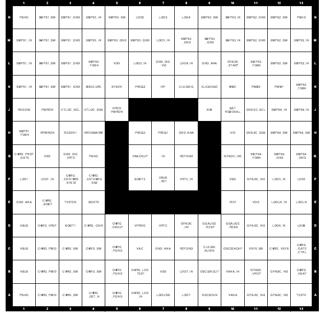 Figure 3-1 Bottom View Ball Mapping
3.2 Pin Attributes
Pin Attributes
| NAME | BALL | TYPE | I/O | DESCRIPTION | CONNECTION IF NOT USED | PULLUP / PULLDOWN |
|---|---|---|---|---|---|---|
| System Supply Regulator/Battery Charger | ||||||
| CHRG_BOOT | E2 | Analog | O | Switched-mode regulator boot-strapped capacitor for the high-side MOSFET gate driver | Floating | – |
| CHRG_CSIN | D4 | Analog | I | Switched-mode regulator current-sense input (without power path) | Ground | – |
| CHRG_CSOUT | D5 | Analog | I | Switched regulator auxiliary power supply, connected to the system supply/battery to provide power in high-impedance mode, switched regulator system/battery voltage/current sense input | System supply | – |
| CHRG_DET_N | A4 | Analog | I | USB charging port detection signal from USB PHY | Ground | – |
| CHRG_EXTCHRG_ENZ | F4 | Digital | O | Output control signal to an external VAC charger (default high) | Floating | – |
| CHRG_EXTCHRG_STATZ | F3 | Digital | I | External VAC charger status input pin | Floating | PU 70 to 190 kΩ |
| CHRG_LED_IN | A6 | Power | I | Input supply for LED indicator | Ground | – |
| CHRG_LED_TEST | B6 | Analog | I/O | External LED driver output | Ground | – |
| CHRG_PGND | A5, B5, C5 | Ground | I | Switched regulator power ground | Ground | – |
| CHRG_PMID | A2, B2, C2 | Analog | O | Switched regulator connection point between reverse blocking MOSFET and high-side switching MOSFET | Floating | – |
| CHRG_SW | A3, B3, C3, B4, C4 | Power | O | Switched regulator output for inductor connection | Floating | – |
| CHRG_VREF | D2 | Analog | O | Switched regulator internal bias regulator voltage | Floating | – |
| VAC | C6 | Power | I | VAC charger input sense line | Ground | – |
| VBUS | B1, C1, D1 | Power | I/O | VBUS input, USB system supply/battery charger power supply | Ground (must be connected to VBUS if VBUS detection from PMIC is needed; for example, USB boot up) | – |
| CHRG_VSYS | C12 | Power | I | System supply | System supply | – |
| CHRG_VBAT | B13 | Power | I/O | Battery voltage for battery charging | System supply | – |
| VBUS_DET | F7 | Digital | O | VBUS detection signal (VSYS level) | Floating | – |
| CHRG_GATE_CTRL | C13 | Analog | O | Control signal for gate of external PMOS (battery switch) | Floating | – |
| CHRG_PROT_GATE | G1 | Analog | O | Control signal for gate of external PMOS to protect against negative input voltage (optional) | Floating | – |
| Power Supplies | ||||||
| GND_ANA | C7, E1, H8, L9 | Ground | I | Analog power ground | Ground | – |
| GND_DIG_VIO | L7 | Ground | I | VIO digital ground | Ground | – |
| GND_DIG_VRTC | G3 | Ground | I | VRTC digital ground | Ground | – |
| PBKG | A1, G4, N1, N13 | Substrate | I | Substrate ground | Ground | – |
| VDD | B7, E11, G2, L5 | Power | I | Analog input voltage supply | System supply | – |
| VIO | H10 | Power | I | The PMIC digital I/O input supply voltage (1.8 V) | N/A | – |
| VPROG | D6 | Power | I | OTP memory programming voltage | Ground | – |
| VBACKUP | G6 | Analog | I | Backup battery connection | Ground | – |
| VSYS_BB | C11 | Power | I | Sense line for system supply | System supply | – |
| Clocking | ||||||
| CLK32KAO | K9 | Digital | O | 32-kHz digital output clock always on when VIO input supply is present | Floating | – |
| CLK32KAUDIO | C9 | Digital | O | 32-kHz digital gated output clock (for example, for audio device) | Floating | – |
| CLK32KG | K8 | Digital | O | 32-kHz digital gated output clock controlled by software | Floating | – |
| OSC32KCAP | C10 | Analog | O | VRTC power supply external filtering capacitor for the 32-kHz crystal oscillator | Floating | – |
| OSC32KIN | A9 | Analog | I | 32-kHz crystal oscillator input or digital clock input | N/A | – |
| OSC32KOUT | B9 | Analog | O | 32-kHz crystal oscillator output or floating in case of digital clock input | N/A or floating | – |
| References | ||||||
| IREF | E10 | Analog | I/O | Reference current generation | N/A | – |
| REFGND | C8, G8 | Ground | I | System reference ground | Ground | – |
| VBG | F10 | Analog | O | Band-gap output reference voltage | N/A | – |
| Testing | ||||||
| TESTEN | E3 | Digital | I | Test mode enable | Ground | PD 170 to 950 kΩ |
| TESTV | A13 | Analog | O | Internal voltages sense line | Floating | – |
| System Control | ||||||
| CTLI2C_SCL | J3 | Digital | I | Control I2C serial clock (external pullup) | N/A | PPU 1.46 to 7.4 kΩ |
| CTLI2C_SDA | J4 | Digital | I/O | Control I2C serial bidirectional data (an external pullup) | N/A | PPU 1.46 to 7.4 kΩ |
| INT | K7 | Digital | O | Maskable interrupt request to the host processor | N/A | – |
| BATREMOVAL | J10 | Digital | O | Battery removal indicator | Floating | – |
| BOOT0 | E4 | Digital | I | Boot ball 0 for power-up sequence selection | Ground or VRTC | – |
| BOOT1 | D3 | Digital | I | Boot ball 1 for power-up sequence selection | Ground or VRTC | – |
| BOOT2 | F6 | Digital | I | Boot ball 2 for power-up sequence selection | Ground or VRTC | – |
| NRESPWRON | J5 | Digital | O | System reset/power-on output | Floating | – |
| NRESWARM | H4 | Digital | I | Warm reset input | Floating | PU 70 to 190 kΩ |
| PREQ1 | H7 | Digital | I | Power request input 1 | Floating | PPU/*PPD 170 to 950 kΩ |
| PREQ2 | K6 | Digital | I | Power request input 2 | Floating | PPU/*PPD 170 to 950 kΩ |
| PREQ3 | H6 | Digital | I | Power request input 3 | Floating | PPU/*PPD 170 to 950 kΩ |
| PWM1 | K12 | Digital | O | Pulse width modulation/general-purpose output 1 | Floating | – |
| PWM2 | K11 | Digital | O | Pulse width modulation/general-purpose output 2 | Floating | – |
| PWRON | J2 | Digital | I | External on-button switch-on event (primary input to launch system wakeup) | N/A | PU 55 to 370 kΩ |
| REGEN1 | H3 | Digital | O | External regulator enable 1 | Floating | – |
| REGEN2 | J1 | Digital | O | External regulator enable 2 | Floating | – |
| RPWRON | H2 | Digital | I | External remote switch-on event (secondary input to launch system wakeup) | Floating | PU 55 to 370 kΩ |
| SYSEN | K5 | Digital | O | External system enable | Floating | – |
| MSECURE | K4 | Digital | I | Secure mode input. Allows I2C access to secure registers | Ground or floating | PD 170 to 950 kΩ |
| DVSI2C_SCL | J11 | Digital | I | DVS I2C serial clock (external pullup) | N/A | PPU 1.46 to 7.4 kΩ |
| DVSI2C_SDA | H11 | Analog | I/O | DVS I2C serial data (external pullup) | N/A | PPU 1.46 to 7.4 kΩ |
| Detection | ||||||
| ID | G7 | Digital | I/O | USB connector identification signal | Floating | – |
| MMC | K10 | Digital | I | MMC card insertion and extraction detection to deactivate the LDO5 regulator | Floating | PPU/*PPD 70 to 190 kΩ |
| SIM | J9 | Power | I | SIM card insertion and extraction detection to deactivate the LDO7 regulator | Floating | PPU/*PPD 70 to 190 kΩ |
| LDO Regulators | ||||||
| VANA | A10 | Power | O | Output voltage for VANA regulator | N/A | – |
| VANA_IN | B10 | Power | I | Input voltage supply for VANA regulator | System supply | – |
| LDO2 | N6 | Power | O | Output voltage for LDO2 regulator | Floating | – |
| LDO2_IN | L6 | Power | I | Input voltage supply for LDO2 regulator | System supply | – |
| LDO4 | N8 | Power | O | Output voltage for LDO4 regulator | Floating | – |
| LDO4_IN | L8 | Power | I | Input voltage supply for LDO4 regulator | System supply | – |
| LDO3 | N7 | Power | O | Output voltage for LDO3 regulator (vibrator driver output) | Floating | – |
| LDO3_IN | M7 | Power | I | Input voltage supply for LDO3 regulator | System supply | – |
| LDO6 | D13 | Power | O | Output voltage for LDO6 regulator | Floating | – |
| LDO6_IN | D12 | Power | I | Input voltage supply for LDO6 regulator | System supply | – |
| LDOLN | E13 | Power | O | Output voltage for LDOLN regulator | Floating | – |
| LDOLN_IN | E12 | Power | I | Input voltage supply for LDOLN regulator | System supply | – |
| LDO5 | F13 | Power | O | Output voltage for LDO5 regulator | Floating | – |
| LDO5_IN | F12 | Power | I | Input voltage supply for LDO5 regulator | System supply | – |
| LDO1 | F1 | Power | O | Output voltage for LDO1 regulator | Floating | – |
| LDO1_IN | F2 | Power | I | Input voltage supply for LDO1 regulator | System supply | – |
| VRTC | D7 | Power | O | Output voltage for VRTC regulator | N/A | – |
| VRTC_IN | F8 | Power | I | Input voltage supply for VRTC regulator | System supply | – |
| LDOUSB | A7 | Power | O | Output voltage for LDOUSB regulator | Floating | – |
| LDO7 | A8 | Power | O | Output voltage for LDO7 regulator | Floating | – |
| LDO7_IN | B8 | Power | I | Input voltage supply for LDO7 regulator | System supply | – |
| Monitoring | ||||||
| GGAUGE_RESN | D10 | Analog | I | Sense resistor input signal negative (ground side) NOTE: Shared with battery charger. |
Ground | – |
| GGAUGE_RESP | D9 | Analog | I | Sense resistor input signal positive (battery negative side) NOTE: Shared with battery charger. |
Ground | – |
| GPADC_IN0 | D11 | Analog | I/O | General-purpose analog-to-digital converter (GPADC) input 0 | Ground | – |
| GPADC_IN1 | D8 | Analog | I/O | GPADC input 1 | Ground | – |
| GPADC_VREF | B11 | Analog | O | GPADC output reference voltage | Floating | – |
| GPADC_IN2 | A12 | Analog | I | GPADC input 2 | Ground | – |
| GPADC_IN3 | B12 | Analog | I/O | GPADC input 3 | Ground | – |
| GPADC_IN4 | A11 | Analog | I/O | GPADC input 4 | Ground | – |
| GPADC_IN5 | G10 | Analog | I | GPADC input 5 | Ground | – |
| GPADC_IN6 | F11 | Analog | I | GPADC input 6 | Ground | – |
| GPADC_START | L10 | Digital | I | Trigger hardware request to start GPADC synchronous conversion | Ground | *PPD 170 to 950 kΩ |
| SMPS Regulators | ||||||
| SMPS4_FDBK | G11 | Analog | I | SMPS4 feedback | Ground | – |
| SMPS4_GND | G12, G13 | Ground | I | SMPS4 ground | Ground | – |
| SMPS4_IN | J12, J13 | Power | I | SMPS4 input voltage | System supply | – |
| SMPS4_SW | H12, H13 | Power | O | SMPS4 switch | Floating | – |
| SMPS2_FDBK | K13 | Analog | I | SMPS2 feedback | Ground | – |
| SMPS2_GND | M11, N11 | Ground | I | SMPS2 ground | Ground | – |
| SMPS2_IN | L13, M13 | Power | I | SMPS2 input voltage | System supply | – |
| SMPS2_SW | L12, M12, N12 | Power | O | SMPS2 switch | Floating | – |
| SMPS3_FDBK | L11 | Analog | I | SMPS3 feedback | Ground | – |
| SMPS3_GND | M8, M9 | Ground | I | SMPS3 ground | Ground | – |
| SMPS3_IN | M10, N10 | Power | I | SMPS3 input voltage | System supply | – |
| SMPS3_SW | N9 | Power | O | SMPS3 switch | Floating | – |
| SMPS1_FDBK | H1 | Analog | I | SMPS1 feedback | Ground | – |
| SMPS1_GND | K3, L3, M3, N3 | Ground | I | SMPS1 ground | Ground | – |
| SMPS1_IN | K1, L1, M1 | Power | I | SMPS1 input voltage | System supply | – |
| SMPS1_SW | K2, L2, M2, N2 | Power | O | SMPS1 switch | Floating | – |
| SMPS5_FDBK | L4 | Analog | I | SMPS5 feedback | Ground | – |
| SMPS5_GND | M5, M6 | Ground | I | SMPS5 ground | Ground | – |
| SMPS5_IN | M4, N4 | Power | I | SMPS5 input voltage | System supply | – |
| SMPS5_SW | N5 | Power | O | SMPS5 switch | Floating | – |