SLVSCN4D October   2014  – June 2019 TPS82084 , TPS82085

PRODUCTION DATA.  

  1. Features
  2. Applications
  3. Description
    1.     Device Images
      1. 1.8 V Output Application
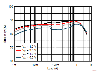
      2. 1.8 V Output Efficiency
  4. Revision History
  5. Pin Configuration and Functions
    1.     Pin Functions
  6. Specifications
    1. 6.1 Absolute Maximum Ratings
    2. 6.2 ESD Ratings
    3. 6.3 Recommend Operating Conditions
    4. 6.4 Thermal Information
    5. 6.5 Electrical Characteristics
    6. 6.6 Typical Characteristics
  7. Detailed Description
    1. 7.1 Overview
    2. 7.2 Functional Block Diagram
    3. 7.3 Feature Description
      1. 7.3.1 Power Save Mode (PSM)
      2. 7.3.2 Low Dropout Operation (100% Duty Cycle)
      3. 7.3.3 Soft Startup
      4. 7.3.4 Switch Current Limit and Short Circuit Protection (Hiccup-Mode)
      5. 7.3.5 Undervoltage Lockout
      6. 7.3.6 Thermal Shutdown
    4. 7.4 Device Functional Modes
      1. 7.4.1 Enable and Disable
      2. 7.4.2 Power Good Output
  8. Application and Implementation
    1. 8.1 Application Information
    2. 8.2 Typical Applications
      1. 8.2.1 1.2-V Output Application
        1. 8.2.1.1 Design Requirements
        2. 8.2.1.2 Detailed Design Procedure
          1. 8.2.1.2.1 Setting the Output Voltage
          2. 8.2.1.2.2 Input and Output Capacitor Selection
        3. 8.2.1.3 Application Performance Curves
  9. Power Supply Recommendations
  10. 10Layout
    1. 10.1 Layout Guidelines
    2. 10.2 Layout Example
    3. 10.3 Thermal Consideration
  11. 11Device and Documentation Support
    1. 11.1 Device Support
      1. 11.1.1 Third-Party Products Disclaimer
    2. 11.2 Related Links
    3. 11.3 Community Resources
    4. 11.4 Trademarks
    5. 11.5 Electrostatic Discharge Caution
    6. 11.6 Glossary
  12. 12Mechanical, Packaging, and Orderable Information
    1. 12.1 Tape and Reel Information

Package Options

Refer to the PDF data sheet for device specific package drawings

Mechanical Data (Package|Pins)
  • SIL|8
Thermal pad, mechanical data (Package|Pins)
Orderable Information

Application Performance Curves

TA = 25°C, VIN = 5 V, VOUT = 1.2 V, BOM = Table 3 unless otherwise noted.
TPS82085 TPS82084 D001_SLVSCN4_TPS82085.gif
VOUT = 1.2 V
Figure 6. Efficiency
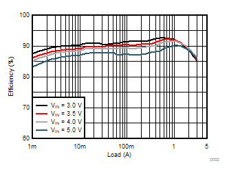
TPS82085 TPS82084 D002_SLVSCN4_TPS82085.gif
VOUT = 1.8 V
Figure 8. Efficiency
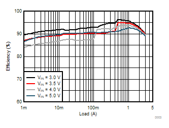
TPS82085 TPS82084 D003_SLVSCN4_TPS82085.gif
VOUT = 2.6 V
Figure 10. Efficiency
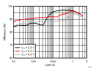
TPS82085 TPS82084 D004_SLVSCN4_TPS82085.gif
VOUT = 3.3 V
Figure 12. Efficiency
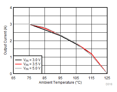
TPS82085 TPS82084 D018_SLVSCN4_TPS82085.gif
VOUT = 1.2 V θJA = 46.6°C/W
Figure 14. Thermal Derating
TPS82085 TPS82084 D005_SLVSCN4_TPS82085.gif
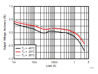
Figure 16. Load Regulation
TPS82085 TPS82084 D007_SLVSCN4_TPS82085.gif
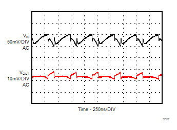
IOUT = 2 A
Figure 18. Input and Output Ripple in PWM Mode
TPS82085 TPS82084 D009_SLVSCN4_TPS82085.gif
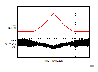
IOUT = 25 mA to 3 A
Figure 20. Load Sweep
TPS82085 TPS82084 D011_SLVSCN4_TPS82085.gif
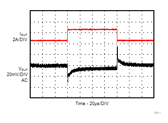
IOUT = 0.5 A to 2.5 A
Figure 22. Load Transient
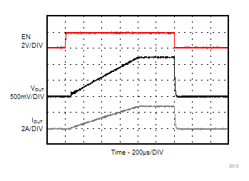
TPS82085 TPS82084 D013_SLVSCN4_TPS82085.gif
Load = 0.4 Ω
Figure 24. Startup / Shutdown with Resistive Load
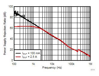
TPS82085 TPS82084 D015_SLVSCN4_TPS82085.gif
Figure 26. Power Supply Rejection Ratio (PSRR)
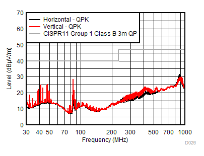
TPS82085 TPS82084 D026_SLVSCN4_TPS82085.gif
RLOAD = 0.47 Ω, VIN = 5 V (battery supply), VOUT = 1.2 V, EMI test board without filters
Figure 28. TPS82085 Radiated Emission
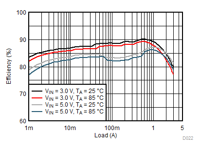
TPS82085 TPS82084 D022_SLVSCN4_TPS82085.gif
VOUT = 1.2 V
Figure 7. Efficiency
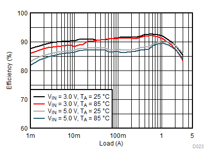
TPS82085 TPS82084 D023_SLVSCN4_TPS82085.gif
VOUT = 1.8 V
Figure 9. Efficiency
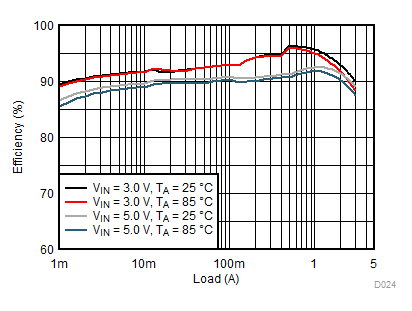
TPS82085 TPS82084 D024_SLVSCN4_TPS82085.gif
VOUT = 2.6 V
Figure 11. Efficiency
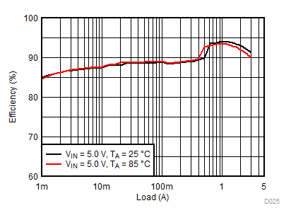
TPS82085 TPS82084 D025_SLVSCN4_TPS82085.gif
VOUT = 3.3 V
Figure 13. Efficiency
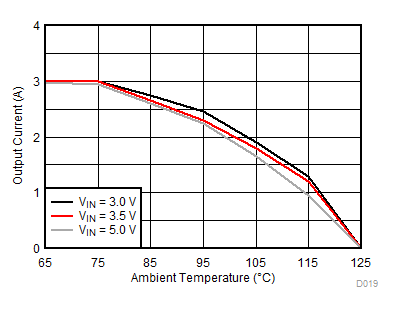
TPS82085 TPS82084 D019_SLVSCN4_TPS82085.gif
VOUT = 2.6 V θJA = 46.6°C/W
Figure 15. Thermal Derating
TPS82085 TPS82084 D006_SLVSCN4_TPS82085.gif
IOUT = 1 A
Figure 17. Line Regulation
TPS82085 TPS82084 D008_SLVSCN4_TPS82085.gif
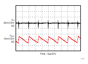
IOUT = 25 mA
Figure 19. Input and Output Ripple in PSM Mode
TPS82085 TPS82084 D010_SLVSCN4_TPS82085.gif
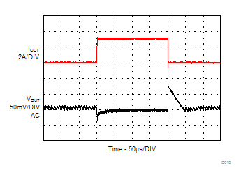
IOUT = 25 mA to 3 A
Figure 21. Load Transient
TPS82085 TPS82084 D012_SLVSCN4_TPS82085.gif
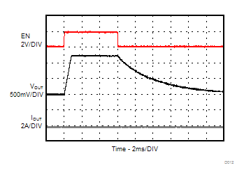
IOUT = no load
Figure 23. Startup / Shutdown without Load
TPS82085 TPS82084 D014_SLVSCN4_TPS82085.gif
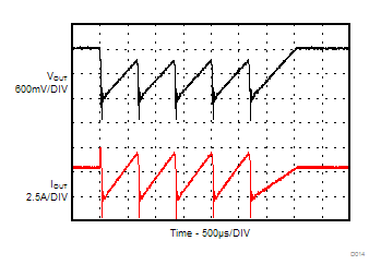
IOUT = 3 A
Figure 25. Short Circuit, HICCUP Protection Entry / Exit
TPS82085 TPS82084 D016_SLVSCN4_TPS82085.gif
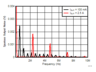
Figure 27. Spurious Output Noise
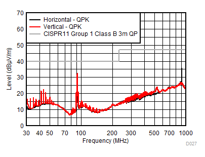
TPS82085 TPS82084 D027_SLVSCN4_TPS82085.gif
RLOAD = 0.68 Ω, VIN = 5 V (battery supply), VOUT = 1.2 V, EMI test board without filters
Figure 29. TPS82084 Radiated Emission