SLVSCY5F February   2016  – January 2023 TPS82130

PRODUCTION DATA  

  1. Features
  2. Applications
  3. Description
  4. Revision History
  5. Pin Configuration and Functions
  6. Specifications
    1. 6.1 Absolute Maximum Ratings
    2. 6.2 ESD Ratings
    3. 6.3 Recommend Operating Conditions
    4. 6.4 Thermal Information
    5. 6.5 Electrical Characteristics
    6. 6.6 Typical Characteristics
  7. Detailed Description
    1. 7.1 Overview
    2. 7.2 Functional Block Diagram
    3. 7.3 Feature Description
      1. 7.3.1 PWM and PSM Operation
      2. 7.3.2 Low Dropout Operation (100% Duty Cycle)
      3. 7.3.3 Switch Current Limit
      4. 7.3.4 Undervoltage Lockout
      5. 7.3.5 Thermal Shutdown
    4. 7.4 Device Functional Modes
      1. 7.4.1 Enable and Disable (EN)
      2. 7.4.2 Soft Start-Up (SS/TR)
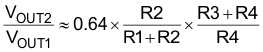
      3. 7.4.3 Voltage Tracking (SS/TR)
      4. 7.4.4 Power-Good Output (PG)
  8. Application and Implementation
    1. 8.1 Application Information
    2. 8.2 Typical Applications
      1. 8.2.1 1.8-V Output Application
        1. 8.2.1.1 Design Requirements
        2. 8.2.1.2 Detailed Design Procedure
          1. 8.2.1.2.1 Custom Design with WEBENCH® Tools
          2. 8.2.1.2.2 Setting the Output Voltage
          3. 8.2.1.2.3 Input and Output Capacitor Selection
          4. 8.2.1.2.4 Soft Start-Up Capacitor Selection
        3. 8.2.1.3 Application Performance Curves
    3. 8.3 Power Supply Recommendations
    4. 8.4 Layout
      1. 8.4.1 Layout Guidelines
      2. 8.4.2 Layout Example
      3. 8.4.3 Thermal Consideration
  9. Device and Documentation Support
    1. 9.1 Device Support
      1. 9.1.1 Development Support
        1. 9.1.1.1 Third-Party Products Disclaimer
        2. 9.1.1.2 Custom Design with WEBENCH® Tools
    2. 9.2 Documentation Support
      1. 9.2.1 Related Documentation
    3. 9.3 Receiving Notification of Documentation Updates
    4. 9.4 Support Resources
    5. 9.5 Trademarks
    6. 9.6 Glossary
    7. 9.7 Electrostatic Discharge Caution
  10. 10Mechanical, Packaging, and Orderable Information

Package Options

Mechanical Data (Package|Pins)
  • SIL|8
Thermal pad, mechanical data (Package|Pins)
Orderable Information

Voltage Tracking (SS/TR)

The SS/TR pin is externally driven by another voltage source to achieve output voltage tracking. The application circuit is shown in Figure 7-1.

GUID-7C3B4206-6DE7-44FD-9B6A-CB044E422352-low.gifFigure 7-1 Output Voltage Tracking

When the SS/TR pin voltage is between 50 mV and 1.2 V, the VOUT2 tracks the VOUT1 as described in Equation 5.

Equation 5. GUID-1A4C065A-2B03-483D-BD93-46A1058378C6-low.gif

When the SS/TR pin voltage is above 1.2 V, the voltage tracking is disabled and the FB pin voltage is regulated at 0.8 V. To decrease the SS/TR pin voltage, the device does not sink current from the output, so the resulting decreases of the output voltage can be slower than the SS/TR pin voltage if the load is light. When driving the SS/TR pin with an external voltage, do not exceed the voltage rating of the SS/TR pin which is VIN + 0.3 V.

Details about tracking and sequencing circuits are found in the Sequencing and Tracking With the TPS621-Family and TPS821-Family Application Report.