SLVSCX6 April 2015 TPS92513 , TPS92513HV
PRODUCTION DATA.
- 1 Features
- 2 Applications
- 3 Description
- 4 Simplified Schematics
- 5 Revision History
- 6 Pin Configuration and Functions
- 7 Specifications
-
8 Detailed Description
- 8.1 Overview
- 8.2 Functional Block Diagram
- 8.3
Feature Description
- 8.3.1 Undervoltage Lockout and Low Power Shutdown (UVLO Pin)
- 8.3.2 Adjustable Switching Frequency (RT/CLK Pin)
- 8.3.3 Synchronizing the Switching Frequency to an External Clock (RT/CLK Pin)
- 8.3.4 Adjustable LED Current (IADJ and ISENSE Pins)
- 8.3.5 PWM Dimming (PDIM Pin)
- 8.3.6 External Compensation (COMP Pin)
- 8.3.7 Overcurrent Protection
- 8.3.8 Overtemperature Protection
- 8.4 Device Functional Modes
-
9 Application and Implementation
- 9.1 Application Information
- 9.2 Typical Application
- 9.3 Design Requirements
- 9.4
Detailed Design Procedure
- 9.4.1 Standard Component Selection
- 9.4.2 Calculate UVLO Resistor Values
- 9.4.3 Calculate the RT Resistor Value (RRT)
- 9.4.4 Calculate the ISENSE Resistor Value (R(ISENSE))
- 9.4.5 Calculate the Inductor Value and Operating Parameters (L)
- 9.4.6 Calculate the Minimum Input Capacitance and the Required RMS Current Rating (CIN)
- 9.4.7 Calculate the Output Capacitor Value (COUT)
- 9.4.8 Calculate the Diode Power Dissipation (D)
- 9.5 Application Curves
- 10Power Supply Recommendations
- 11Layout
- 12Device and Documentation Support
- 13Mechanical, Packaging, and Orderable Information
Package Options
Mechanical Data (Package|Pins)
- DGQ|10
Thermal pad, mechanical data (Package|Pins)
- DGQ|10
Orderable Information
11 Layout
The TPS92513 requires a proper layout for optimal performance. The following section gives some guidelines to ensure a proper layout.
11.1 Layout Guidelines
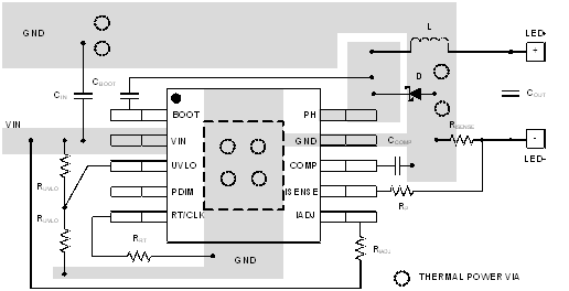
An example of a proper layout for the TPS92513 is shown in Figure 17. Creating a large GND plane under the integrated circuit (IC) for good electrical and thermal performance is important.
- The GND pin of the device must connect to the GND plane directly beneath the IC.
- Thermal vias can be used to connect the topside GND plane to additional printed-circuit board (PCB) layers for heat spreading and more solid grounding.
- The input capacitors must be located as close as possible to the VIN pin and the GND plane and should be tied to a solid backside ground plane using multiple vias.
- The compensation components must be located as close as possible to the COMP and GND pins in order to minimize noise sensitivity.
- The PH trace must be kept as short as possible to reduce the possibility of radiated noise/EMI.
- The ISENSE node should be kept as short as possible and shielded from noise.
- The RT/CLK pin is sensitive and its routing must be kept as short as possible.
- In higher current applications, routing the load current of the current-sense resistor to the junction of the input capacitor and rectifier diode GND node may be necessary. The easiest way to accomplish this is to use a backside ground plane and arrays of vias to connect the top side ground connections solidly to the backside plane. This steers the high current away from the sensitive RT/CLK to GND connection.
- If possible, the current loop created when the internal MOSFET is on should be in the same direction as the current loop when the internal MOSFET is off and the schottky diode is conducting. This will prevent magnetic field reversal, reduce radiated noise, and simplify EMI filtering.
11.2 Layout Example
 Figure 17. Layout Example