SLVSCX6 April 2015 TPS92513 , TPS92513HV
PRODUCTION DATA.
- 1 Features
- 2 Applications
- 3 Description
- 4 Simplified Schematics
- 5 Revision History
- 6 Pin Configuration and Functions
- 7 Specifications
-
8 Detailed Description
- 8.1 Overview
- 8.2 Functional Block Diagram
- 8.3
Feature Description
- 8.3.1 Undervoltage Lockout and Low Power Shutdown (UVLO Pin)
- 8.3.2 Adjustable Switching Frequency (RT/CLK Pin)
- 8.3.3 Synchronizing the Switching Frequency to an External Clock (RT/CLK Pin)
- 8.3.4 Adjustable LED Current (IADJ and ISENSE Pins)
- 8.3.5 PWM Dimming (PDIM Pin)
- 8.3.6 External Compensation (COMP Pin)
- 8.3.7 Overcurrent Protection
- 8.3.8 Overtemperature Protection
- 8.4 Device Functional Modes
-
9 Application and Implementation
- 9.1 Application Information
- 9.2 Typical Application
- 9.3 Design Requirements
- 9.4
Detailed Design Procedure
- 9.4.1 Standard Component Selection
- 9.4.2 Calculate UVLO Resistor Values
- 9.4.3 Calculate the RT Resistor Value (RRT)
- 9.4.4 Calculate the ISENSE Resistor Value (R(ISENSE))
- 9.4.5 Calculate the Inductor Value and Operating Parameters (L)
- 9.4.6 Calculate the Minimum Input Capacitance and the Required RMS Current Rating (CIN)
- 9.4.7 Calculate the Output Capacitor Value (COUT)
- 9.4.8 Calculate the Diode Power Dissipation (D)
- 9.5 Application Curves
- 10Power Supply Recommendations
- 11Layout
- 12Device and Documentation Support
- 13Mechanical, Packaging, and Orderable Information
Package Options
Mechanical Data (Package|Pins)
- DGQ|10
Thermal pad, mechanical data (Package|Pins)
- DGQ|10
Orderable Information
7 Specifications
7.1 Absolute Maximum Ratings
over operating free-air temperature range (unless otherwise noted) (1)| MIN | MAX | UNIT | |||
|---|---|---|---|---|---|
| Input voltage | VIN (TPS92513HV) | –0.3 | 65 | V | |
| VIN (TPS92513) | –0.3 | 45 | |||
| PDIM, UVLO | –0.3 | 5 | |||
| BOOT | (PH + 8) | ||||
| ISENSE, IADJ, COMP | –0.3 | 3 | |||
| RT/CLK | –0.3 | 3.6 | |||
| Output voltage | PH (TPS92513HV) | –0.6 | 65 | V | |
| PH (TPS92513) | –0.6 | 45 | |||
| PH, 10-ns Transient | –2 | ||||
| Voltage Difference | PAD to GND | ±200 | mV | ||
| Source Current | PH | Current Limit | A | ||
| Sink current | VIN | Current Limit | A | ||
| BOOT | 1 | mA | |||
| TJ | Operating junction temperature | –40 | 150 | °C | |
| Tstg | Storage temperature | –65 | 150 | °C | |
(1) Stresses beyond those listed under Absolute Maximum Ratings may cause permanent damage to the device. These are stress ratings only, which do not imply functional operation of the device at these or any other conditions beyond those indicated under Recommended Operating Conditions. Exposure to absolute-maximum-rated conditions for extended periods may affect device reliability.
7.2 ESD Ratings
| VALUE | UNIT | |||
|---|---|---|---|---|
| V(ESD) | Electrostatic discharge | Human-body model (HBM),ESD stress voltage(1) | ±2000 | V |
| Charged-device model (CDM), ESD stress voltage(2) | ±500 | V | ||
(1) JEDEC document JEP155 states that 500-V HBM allows safe manufacturing with a standard ESD control process. Manufacturing with less than 500-V HBM is possible with the necessary precautions. Pins listed as ±2 kV may actually have higher performance.
(2) JEDEC document JEP157 states that 250-V CDM allows safe manufacturing with a standard ESD control process. Manufacturing with less than 250-V CDM is possible with the necessary precautions. Pins listed as ±500 V may actually have higher performance.
7.3 Recommended Operating Conditions
over operating free-air temperature range (unless otherwise noted)| MIN | MAX | UNIT | ||
|---|---|---|---|---|
| VIN | Input voltage (TPS92513HV) | 4.5 | 60 | V |
| Input voltage (TPS92513) | 4.5 | 42 | ||
| fSW | Switching frequency range using RT mode | 100 | 2000 | kHz |
| Switching frequency range using CLK mode | 300 | 2000 | ||
| tMIN(RT/CLK) | Minimum RT/CLK input pulse width for switching frequency synchronization | 51 | ns | |
| TJ | Operating junction temperature | –40 | 125 | °C |
7.4 Thermal Information
| THERMAL METRIC(1) | TPS92513 TPS92513HV |
UNIT | |
|---|---|---|---|
| DGQ (10 PINS) | |||
| RθJA | Junction-to-ambient thermal resistance | 66.7 | °C/W |
| RθJC(top) | Junction-to-case (top) thermal resistance | 45.8 | |
| RθJB | Junction-to-board thermal resistance | 37.5 | |
| ψJT | Junction-to-top characterization parameter | 1.8 | |
| ψJB | Junction-to-board characterization parameter | 37.1 | |
| RθJC(bot) | Junction-to-case (bottom) thermal resistance | 15.4 | |
(1) For more information about traditional and new thermal metrics, see the IC Package Thermal Metrics application report, SPRA953.
7.5 Electrical Characteristics
–40°C ≤ TJ ≤ 125°C, VVIN = 12V (unless otherwise noted)| PARAMETER | TEST CONDITIONS | MIN | TYP | MAX | UNIT | |
|---|---|---|---|---|---|---|
| SUPPLY VOLTAGE (VIN) | ||||||
| VINUVLO | VIN undervoltage lockout threshold | No voltage hysteresis, rising and falling | 2.94 | V | ||
| IVINSD | Shutdown supply current | VUVLO = 0 V, 4.5 V ≤ VVIN ≤ 42 V (60 V for HV) | 11.5 | µA | ||
| IVIN | Non-switching supply current | VISENSE = 220 mV, 4.5V ≤ VVIN ≤ 42 V (60 V for HV) | 337 | 407 | µA | |
| UNDER VOLTAGE LOCKOUT (UVLO) | ||||||
| VUVLO | UVLO threshold voltage | Rising threshold | 1.12 | 1.22 | 1.30 | V |
| UVLO pin source current | VUVLO = 1.5 V (device enabled) | 3.97 | µA | |||
| VUVLO = 1 V (device disabled) | 1.05 | |||||
| ANALOG CURRENT ADJUST (VIADJ, VISENSE) | ||||||
| VIADJ | IADJ clamp voltage | IIADJ = 1 µA | 1.8 | V | ||
| IIADJ = 100 µA | 2.77 | |||||
| VISENSE | Current sense voltage | VIADJ = 1.2 V, TJ = 25°C to 125°C | 191 | 200 | 210 | mV |
| VIADJ = 0.18 V, TJ = 25°C to 125°C | 21.4 | 30.0 | 40.0 | |||
| IIADJ = 1 µA, TJ = 25°C to 125°C | 285 | 300 | 309 | |||
| IIADJ = 100 µA, TJ = 25°C to 125°C | 286 | 300 | 309 | |||
| Current sense voltage level | 180 mV ≤ VIADJ ≤ 1.8V | VIADJ/6 | ||||
| HIGH-SIDE MOSFET (BOOT, PH) | ||||||
| RDS(on) | On-resistance | VVIN = 4.5 V, (VBOOT – VPH) = 3.5 V | 255 | mΩ | ||
| (VBOOT – VPH) = 6 V | 220 | 375 | ||||
| VBOOT | BOOT-PH voltage | VPDIM = 3V | 6 | V | ||
| IBOOT | BOOT-PH current | VPDIM = 0V, (VBOOT – VPH) = 5V | 93.9 | µA | ||
| VBOOTUV | BOOT-PH under voltage lockout | Rising threshold | 2.25 | 2.81 | V | |
| Falling threshold | 1.42 | 1.99 | ||||
| tON(min) | Minimum on time | VCOMP = 0 | 140 | ns | ||
| ERROR AMPLIFIER (ISENSE, COMP) | ||||||
| Input bias current | VISENSE = 200 mV | 20 | nA | |||
| gM(ea) | Transconductance gain | VIADJ = 1.2 V, 180 mV < VISENSE < 220 mV, VCOMP = 1 V | 331 | µA/V | ||
| DC gain | VIADJ = 1.2 V , VISENSE = 0.2 V | 10 | kV/V | |||
| Bandwidth | 2.7 | MHz | ||||
| Source/sink current | VIADJ = 1.2 V , VCOMP = 1 V, VISENSE = 200 mV ± 100 mV |
±28 | µA | |||
| CURRENT LIMIT | ||||||
| Current limit threshold | 6 | A | ||||
| THERMAL SHUTDOWN | ||||||
| TSD | Thermal shutdown | 165 | °C | |||
| Thermal shutdown hysteresis | 20 | |||||
| TIMING RESISTOR AND EXTERNAL CLOCK (RT/CLK) | ||||||
| VRT | RT/CLK regulated voltage | RRT = 200 kΩ | 474 | 500 | 513 | mV |
| fSW | Switching frequency | VVIN = 6 V, RRT = 200 kΩ | 447 | 557 | 648 | kHz |
| RT/CLK high threshold | VVIN = 6 V | 1.49 | 1.81 | V | ||
| RT/CLK low threshold | VVIN = 6 V | 0.63 | 1.02 | V | ||
| PWM DIMMING (PDIM) | ||||||
| IPDIM | PDIM source current | VPDIM = 0 | 1.04 | µA | ||
| VIH | High-level input voltage | 1.34 | 1.45 | V | ||
| VIL | Low-level input voltage | 0.79 | 0.88 | |||
7.6 Timing Requirements
| MIN | NOM | MAX | UNIT | |||
|---|---|---|---|---|---|---|
| TIMING RESISTOR AND EXTERNAL CLOCK (RT/CLK) | ||||||
| RT/CLK falling edge to PH rising edge delay | Measured at 500 kHz with RT resistor in series, VVIN = 6 V | 92.1 | ns | |||
| Phase loop (PLL) lock-in time | fSW = 500 kHz | 100 | µs | |||
| PWM DIMMING (PDIM) | ||||||
| tRISE | Rising propagation delay | 305 | ns | |||
| tFALL | Falling propagation delay | 535 | ||||
7.7 Typical Characteristics
VIN = 24V, Unless otherwise specified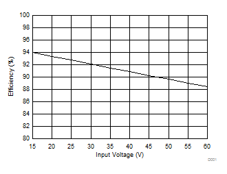
| 1.5 A LED Current | 4 LEDs in Series | VIADJ = 1.8 V |
| fSW = 570 kHz | VOUT = 13.1 V |
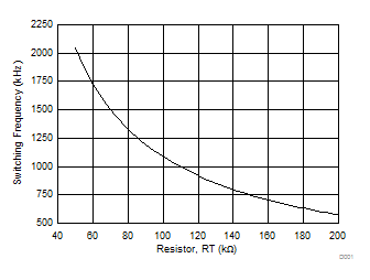
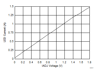
| 1.5 A LED Current | 3 LEDs in Series | |
| VOUT = 9.9 V |

| VIN = 12 V | ||
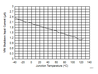
A.
Figure 9. Shutdown Input Current vs Junction Temperature
| VVIN = 12 V | ||
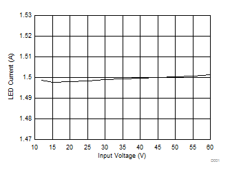
| 1.5 A LED Current | 3 LEDs in Series | VIADJ = 1.8 V |
| VOUT = 9.9 V |
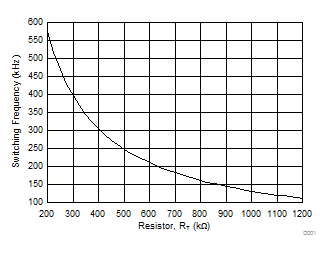
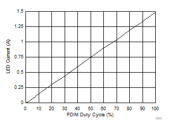
| 1.5 A LED Current | 3 LEDs in Series | VIADJ = 1.8 V |
| 250 Hz PWM Frequency | VOUT = 9.9 V |
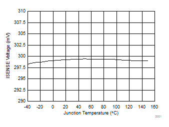
| VIADJ = 1.8 V | ||
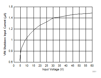
A.
Figure 10. Shutdown Input Current vs Input Voltage
| TJ = 25°C | ||