SLVSFG3 April 2020 TPS92612
PRODUCTION DATA.
- 1 Features
- 2 Applications
- 3 Description
- 4 Revision History
- 5 Pin Configuration and Functions
- 6 Specifications
- 7 Detailed Description
- 8 Application and Implementation
- 9 Power Supply Recommendations
- 10Layout
- 11Device and Documentation Support
- 12Mechanical, Packaging, and Orderable Information
Package Options
Mechanical Data (Package|Pins)
- DBV|5
Thermal pad, mechanical data (Package|Pins)
Orderable Information
8.2.2.2 Detailed Design Procedure
In linear LED driver applications, the input and output voltage variation generates the most of the thermal concerns. The resistor current I(P), as indicated by Ohm's law, depends on the voltage across the external resistors. The TPS92612 controls the driver current I(DRIVE) to attain the desired total current. If I(P) increases, the TPS92612 device decreases I(DRIVE) to compensate, and vice versa. The parallel-resistor takes highest current and generates maximum heat at maximum supply voltage and minimum LED-string forward voltage.
The parallel resistor value must be carefully calculated to ensure that 1) thermal dissipation for both the TPS92612 device and the resistor is within their thermal dissipation limits, and 2) device current at high voltage drop condition is above the minimal output-current requirement.
STEP 1: Determine the current setting resistor, R(SNS) value by using Equation 4.

where
- V(CS_REG) = 98 mV (typical)
- I(LED) = 150 mA
The calculated result for R(SNS) is 0.653 Ω.
STEP 2: Calculate the parallel resistor, R(P) value by using Equation 5.
The parallel resistor R(P) is recommended to consume 50% of the total current at maximum supply voltage and minimum LED-string forward voltage.

where
- V(CS_REG) = 98 mV (typical)
- I(LED) = 150 mA
The calculated result for R(P) is about 100 Ω at V(SUPPLY) = 13.2 V.
STEP 3: Power consumption analysis for the worst application conditions.
The total device power consumption can be calculated by Equation 6.

where
- V(CS_REG) = 98 mV (typical)
- I(Quiescent) = 250 µA (maximum)
The calculated maximum power consumption on the TPS92612 device is 0.566 W at V(SUPPLY) = 13.2 V, V(OUT) = 3 × 1.9 V = 5.7 V and I(LED) = 150 mA.
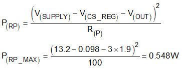
The power consumption on resistor R(P) can be calculated through Equation 7.

where
- V(CS_REG) = 98 mV (typical)
The calculated maximum power consumption on the 100 Ω, R(P) parallel resistor is 0.548 W at V(SUPPLY) = 13.2 V and V(OUT) = 3 × 1.9 V = 5.7 V.
TI recommends adding capacitors C(SUPPLY) at SUPPLY and C(OUT) at OUT. One 1-μF capacitor plus one 100-nF decoupling ceramic capacitor close to the SUPPLY pin is recommended for C(SUPPLY), and a 10-nF ceramic capacitor close to the OUT pin is recommended for C(OUT). The larger capacitor for C(SUPPLY) or C(OUT) is helpful for EMI and ESD immunity, however large C(OUT) takes a longer time to charge up the capacitor and could affect PWM dimming performance.
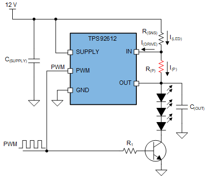
Note that the parallel resistor path cannot be shut down by PWM or fault protection. If PWM control is required, TI recommends an application circuit as shown in Figure 16. A NPN bipolar transistor with a base current-limiting resistor, R1, can modulate the output current together with the device PWM function. The resistor value of R1 needs to be calculated based on the applied PWM voltage and β value of selected NPN transistor.
 Figure 16. PWM Control With Heat Sharing Resistor