SLVSEC4B April   2019  – January 2020 TPS92613-Q1

PRODUCTION DATA.  

  1. Features
  2. Applications
  3. Description
    1.     Device Images
      1.      Typical Application Diagram
  4. Revision History
  5. Pin Configuration and Functions
    1.     Pin Functions
  6. Specifications
    1. 6.1 Absolute Maximum Ratings
    2. 6.2 ESD Ratings
    3. 6.3 Recommended Operating Conditions
    4. 6.4 Thermal Information
    5. 6.5 Electrical Characteristics
    6. 6.6 Timing Requirements
    7. 6.7 Typical Characteristics
  7. Detailed Description
    1. 7.1 Overview
    2. 7.2 Functional Block Diagram
    3. 7.3 Feature Description
      1. 7.3.1 Power Supply
        1. 7.3.1.1 Power-On Reset (POR)
        2. 7.3.1.2 Low-Quiescent-Current
      2. 7.3.2 Constant-Current Driver
      3. 7.3.3 PWM Control
      4. 7.3.4 Supply Control
      5. 7.3.5 Diagnostics and Protection
        1. 7.3.5.1 Open-Circuit Detection
        2. 7.3.5.2 Short-to-GND Detection
        3. 7.3.5.3 Overtemperature Protection
        4. 7.3.5.4 DIAGEN
        5. 7.3.5.5 Low-Dropout Operation
      6. 7.3.6 FAULT Bus Output With One-Fails–All-Fail
      7. 7.3.7 Fault Table
    4. 7.4 Device Functional Modes
      1. 7.4.1 Undervoltage Lockout, V(SUPPLY) < V(POR_rising)
      2. 7.4.2 Normal Operation V(SUPPLY) ≥ 4.5 V
      3. 7.4.3 Low-Voltage Dropout Operation
      4. 7.4.4 Fault Mode
  8. Application and Implementation
    1. 8.1 Application Information
    2. 8.2 Typical Applications
      1. 8.2.1 Single-Channel LED Driver With Diagnostics
        1. 8.2.1.1 Design Requirements
        2. 8.2.1.2 Detailed Design Procedure
        3. 8.2.1.3 Application Curves
      2. 8.2.2 Single-Channel LED Driver With Heat Sharing
        1. 8.2.2.1 Design Requirements
        2. 8.2.2.2 Detailed Design Procedure
        3. 8.2.2.3 Application Curves
  9. Power Supply Recommendations
  10. 10Layout
    1. 10.1 Layout Guidelines
    2. 10.2 Layout Example
  11. 11Device and Documentation Support
    1. 11.1 Documentation Support
      1. 11.1.1 Related Documentation
    2. 11.2 Receiving Notification of Documentation Updates
    3. 11.3 Support Resources
    4. 11.4 Trademarks
    5. 11.5 Electrostatic Discharge Caution
    6. 11.6 Glossary
  12. 12Mechanical, Packaging, and Orderable Information

Package Options

Mechanical Data (Package|Pins)
Thermal pad, mechanical data (Package|Pins)
Orderable Information

PWM Control

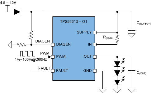
The pulse width modulation (PWM) input of the TPS92613-Q1 functions as enable for the output current. When the voltage applied on the PWM pin is higher than VIH(PWM), the output current is enabled. When the voltage applied on PWM pin is lower than VIL(PWM), the output current is disabled as well as the diagnostic features. Besides output current enable and disable function, the PWM input of TPS92613-Q1 also supports adjustment of the average current output for brightness control if the frequency of applied PWM signal is higher than 100 Hz, which is out of visible frequency range of human eyes. TI recommends a 200-Hz PWM signal with 1% to 100% duty cycle input for brightness control. See to Figure 20 for typical PWM dimming application.
TPS92613-Q1 schem-04-slvsec4.gifFigure 20. Typical Application Schematic for PWM Dimming