SLVSGJ5 April 2022 TPSM63604
PRODUCTION DATA
- 1 Features
- 2 Applications
- 3 Description
- 4 Revision History
- 5 Device Comparison Table
- 6 Pin Configuration and Functions
- 7 Specifications
-
8 Detailed Description
- 8.1 Overview
- 8.2 Functional Block Diagram
- 8.3
Feature Description
- 8.3.1 Input Voltage Range (VIN1, VIN2)
- 8.3.2 Adjustable Output Voltage (FB)
- 8.3.3 Input Capacitors
- 8.3.4 Output Capacitors
- 8.3.5 Switching Frequency (RT)
- 8.3.6 Precision Enable and Input Voltage UVLO (EN/SYNC)
- 8.3.7 Frequency Synchronization (EN/SYNC)
- 8.3.8 Power Good Monitor (PG)
- 8.3.9 Adjustable Switch-Node Slew Rate (RBOOT, CBOOT)
- 8.3.10 Bias Supply Regulator (VCC, VLDOIN)
- 8.3.11 Overcurrent Protection (OCP)
- 8.3.12 Thermal Shutdown
- 8.4 Device Functional Modes
-
9 Applications and Implementation
- 9.1 Application Information
- 9.2
Typical Applications
- 9.2.1 Design 1 – High-Efficiency 4-A Synchronous Buck Regulator for Industrial Applications
- 9.2.2 Design 2 – Inverting Buck-Boost Regulator with Negative Output Voltage
- 10Power Supply Recommendations
- 11Layout
- 12Device and Documentation Support
- 13Mechanical, Packaging, and Orderable Information
Package Options
Mechanical Data (Package|Pins)
- RDL|20
Thermal pad, mechanical data (Package|Pins)
Orderable Information
8.3.3 Input Capacitors
Input capacitors are necessary to limit the input ripple voltage to the module due to switching frequency AC currents. TI recommends using ceramic capacitors to provide low impedance and high RMS current rating over a wide temperature range. Equation 2 gives the input capacitor RMS current. The highest input capacitor RMS current occurs at D = 0.5, at which point, the RMS current rating of the capacitors should be greater than half the output current.
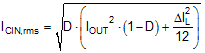
where
- D = VOUT / VIN is the module duty cycle.
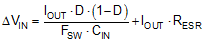
Ideally, the DC and AC components of input current to the buck stage are provided by the input voltage source and the input capacitors, respectively. Neglecting inductor ripple current, the input capacitors source current of amplitude (IOUT – IIN) during the D interval and sink IIN during the 1 – D interval. Thus, the input capacitors conduct a square-wave current of peak-to-peak amplitude equal to the output current. The resultant capacitive component of AC ripple voltage is a triangular waveform. Together with the ESR-related ripple component, Equation 3 gives the peak-to-peak ripple voltage amplitude:
Equation 4 gives the input capacitance required for a particular load current:
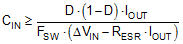
where
- ΔVIN is the input voltage ripple specification.
The TPSM63604 requires a minimum of two 10-µF ceramic input capacitors, preferably with X7R or X7S dielectric and in 1206 or 1210 footprint. Additional capacitance can be required for applications to meet conducted EMI specifications, such as CISPR 11 or CISPR 32.
Table 8-2 includes a preferred list of capacitors by vendor. To minimize the parasitic inductance in the switching loops, position the ceramic input capacitors in a symmetrical layout close to the VIN1 and VIN2 pins and connect the capacitor return terminals to the PGND pins using a copper ground plane under the module.
| Vendor(1) | Dielectric | Part Number | Case Size | Capacitance (µF)(2) | Rated Voltage (V) |
|---|---|---|---|---|---|
| TDK | X7R | C3216X7R1H106K160AC | 1206 | 10 | 50 |
| Murata | X7S | GCM32EC71H106KA03K | 1210 | 10 | 50 |
| AVX | X7R | 12105C106MAT2A | 1210 | 10 | 50 |
| Murata | X7R | GRM32ER71H106KA12L | 1210 | 10 | 50 |
As discussed in Section 10, an electrolytic bulk capacitance (68 µF to 100 µF) provides low-frequency filtering and parallel damping to mitigate the effects of input parasitic inductance resonating with the low-ESR, high-Q ceramic input capacitors.