SLUSDN6A September 2019 – December 2020 TPSM82810 , TPSM82813
PRODUCTION DATA
- 1 Features
- 2 Applications
- 3 Description
- 4 Revision History
- 5 Device Comparison Table
- 6 Pin Configuration and Functions
- 7 Specifications
- 8 Parameter Measurement Information
- 9 Detailed Description
- 10Application and Implementation
- 11Power Supply Recommendations
- 12Layout
- 13Device and Documentation Support
- 14Mechanical, Packaging, and Orderable Information
Package Options
Mechanical Data (Package|Pins)
- SIL|14
Thermal pad, mechanical data (Package|Pins)
Orderable Information
3 Description
TPSM8281x is a family of pin-to-pin 3-A and 4-A compatible high efficiency and easy to use synchronous step-down DC/DC power modules with integrated inductors. They are based on a fixed-frequency peak current-mode control topology. They are used in telecommunication, test and measurement, and medical applications with high power density and ease of use requirements. Low resistance switches allow up to 4-A continuous output current at high ambient temperatures. The switching frequency is externally adjustable from 1.8 MHz to 4 MHz and can also be synchronized to an external clock in the same frequency range. In PFM/PWM mode, the TPSM8281x automatically enters Power Save Mode at light loads to maintain high efficiency across the whole load range. The TPSM8281x provides a 1% output voltage accuracy in PWM mode which helps design a power supply with high output voltage accuracy. The SS/TR pin sets the start-up time or tracks the output voltage to an external source. This allows external sequencing of different supply rails and limits the inrush current during start-up.
| PART NUMBER | PACKAGE(1) | BODY SIZE (NOM) |
|---|---|---|
| TPSM82810 | µSiL | 3-mm x 4-mm x 2.4-mm |
| TPSM82813 | µSiL | 3-mm x 4-mm x 2.4-mm |
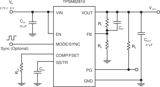
 Schematic
 Efficiency vs
Output Current; VIN = 5 V;
Efficiency vs
Output Current; VIN = 5 V;PFM; fS = 1.8 MHz; TA = 25°C