SLUSDN6A September 2019 – December 2020 TPSM82810 , TPSM82813
PRODUCTION DATA
- 1 Features
- 2 Applications
- 3 Description
- 4 Revision History
- 5 Device Comparison Table
- 6 Pin Configuration and Functions
- 7 Specifications
- 8 Parameter Measurement Information
- 9 Detailed Description
- 10Application and Implementation
- 11Power Supply Recommendations
- 12Layout
- 13Device and Documentation Support
- 14Mechanical, Packaging, and Orderable Information
Package Options
Mechanical Data (Package|Pins)
- SIL|14
Thermal pad, mechanical data (Package|Pins)
Orderable Information
9.4.4 Current Limit and Short Circuit Protection
The TPSM8281x is protected against overload and short circuit events. If the inductor current exceeds the current limit ILIMH, the high-side MOSFET is turned off and the low-side MOSFET is turned on to ramp down the inductor current. The high-side MOSFET turns on again only if the current in the low-side MOSFET has decreased below the low-side current limit. Due to internal propagation delays, the actual current can exceed the static current limit. The dynamic current limit is given as:
Equation 7. 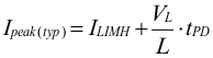
where
- ILIMH is the static current limit, as specified in the electrical characteristics
- L is the effective inductance (typically 470 nH)
- VL is the voltage across the inductor (VIN - VOUT)
- tPD is the internal propagation delay of typically 50 ns
The dynamic peak current is calculated as follows:
Equation 8. 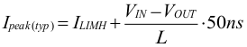
The low-side MOSFET also contains a negative current limit to prevent excessive current from flowing back through the inductor to the input. If the low-side sinking current limit is exceeded, the low-side MOSFET is turned off. In this scenario, both MOSFETs are off until the start of the next cycle. The negative current limit is only active in Forced PWM mode.