SLVSG68 November 2022 TPSM82901
PRODUCTION DATA
- 1 Features
- 2 Applications
- 3 Description
- 4 Revision History
- 5 Pin Configuration and Functions
- 6 Specifications
-
7 Detailed Description
- 7.1 Overview
- 7.2 Functional Block Diagram
- 7.3
Feature Description
- 7.3.1 Mode Selection and Device Configuration (MODE/S-CONF)
- 7.3.2 Adjustable VO Operation (External Voltage Divider)
- 7.3.3 Setable VO Operation (VSET and Internal Voltage Divider)
- 7.3.4 Soft Start/Tracking (SS/TR)
- 7.3.5 Smart Enable with Precise Threshold
- 7.3.6 Power Good (PG)
- 7.3.7 Undervoltage Lockout (UVLO)
- 7.3.8 Current Limit And Short Circuit Protection
- 7.3.9 Thermal Shutdown
- 7.4 Device Functional Modes
- 8 Application and Implementation
- 9 Device and Documentation Support
- 10Mechanical, Packaging, and Orderable Information
Package Options
Mechanical Data (Package|Pins)
- SIS|11
Thermal pad, mechanical data (Package|Pins)
Orderable Information
8.2.2.3.3 Soft-Start Capacitor
A capacitor connected between SS/TR pin and GND allows a user-programmable start-up slope of the output voltage.
 Figure 8-2 Soft-Start Operation Simplified Schematic
An internal constant current source is provided to charge the external capacitance. The capacitor required for a given soft-start ramp time is given by:
Equation 11. 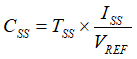
where
- CSS is the capacitance required at the SS/TR pin.
- TSS is the desired soft-start ramp time.
- ISS is the SS/TR source current, see the Electrical Characteristics.
- VREF is the feedback regulation voltage divided by tracking gain (VFB/0.75), see the Electrical Characteristics.
The fastest achievable typical ramp time is 150 µs even if the external Css capacitance is lower than 680 pF or the pin is open.