SLUSCV7A July 2017 – August 2017 TPSM84203 , TPSM84205 , TPSM84212
PRODUCTION DATA.
- 1 Features
- 2 Applications
- 3 Description
- 4 Revision History
- 5 Pin Configuration and Functions
- 6 Specifications
- 7 Detailed Description
- 8 Application and Implementation
- 9 Power Supply Recommendations
- 10Layout
- 11Device and Documentation Support
- 12Mechanical, Packaging, and Orderable Information
Package Options
Mechanical Data (Package|Pins)
- EAB|3
Thermal pad, mechanical data (Package|Pins)
Orderable Information
1 Features
- Complete Integrated Power Solution
- 3-Pin TO-220 Footprint
- Efficiencies up to 95%
- Fixed Output Voltage Options:
3.3 V, 5 V, and 12 V - 400-kHz Switching Frequency
- Advanced Eco-mode™ Pulse Skip
- Pre-bias Output Start-up
- Over-Current Protection
- Output Over-Voltage Protection
- Thermal Shutdown
- Operating Junction Range: –40°C to +125°C
- Operating Ambient Range: –40°C to +85°C
- Meets EN55022 Class B Emissions
- Create a Custom Design Using the TPSM84203 with the WEBENCH® Power Designer
2 Applications
- 12-V, 24-V Distributed Power-Bus Supply
- Industrial White Goods
- Consumer
- Audio
- STB, DTV
- Printer
3 Description
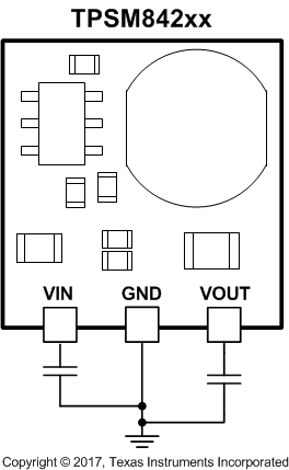
The TPSM842xx power module is an easy-to-use integrated power solution that combines a 1.5-A DC/DC converter with power MOSFETs, an inductor, and passives into a 3-pin, through-hole package. This total power solution requires adding only input and output capacitors and eliminates the loop compensation and magnetics part selection from the design process.
The standard TO-220 pin-out allows a much improved replacement of linear regulators packaged in this industry standard footprint. The TPSM842xx devices provide much higher efficiency without the need of a heatsink.
Device Information(1)
| PART NUMBER | PACKAGE | BODY SIZE (NOM) |
|---|---|---|
| TPSM84203 | EAB | 10 mm x 11 mm |
| TPSM84205 | ||
| TPSM84212 |
- For all available packages, see the orderable addendum at the end of the data sheet.
Device Comparison
| PART NUMBER | OUTPUT VOLTAGE |
|---|---|
| TPSM84203 | 3.3 V |
| TPSM84205 | 5.0 V |
| TPSM84212 | 12.0 V |
Simplified Application
