6 Specifications
6.1 Absolute Maximum Ratings
Over operating free-air temperature range (unless otherwise noted)(1)
| PARAMETER |
MIN |
MAX |
UNIT |
| Input Voltage |
|
–0.3 |
30 |
V |
| Output Voltage |
TPSM84203 |
–0.3 |
3.9 |
V |
| TPSM84205 |
–0.3 |
5.7 |
V |
| TPSM84212 |
–0.3 |
13.0 |
V |
| Mechanical Shock |
Mil-STD-883D, Method 2002.3, 1msec, 1/2 sine, mounted |
|
1500 |
G |
| Mechanical Vibration |
Mil-STD-883D, Method 2007.2, 20-2000Hz |
|
10 |
G |
| Operating IC Junction Temperature range, TJ (2) |
–40 |
125 |
°C |
| Operating Ambient Temperature range, TA (2) |
–40 |
85 |
°C |
| Storage temperature, Tstg |
–60 |
150 |
°C |
(1) Stresses beyond those listed under Absolute Maximum Ratings may cause permanent damage to the device. These are stress ratings only, which do not imply functional operation of the device at these or any other conditions beyond those indicated under Recommended Operating Conditions. Exposure to absolute-maximum-rated conditions for extended periods may affect device reliability.
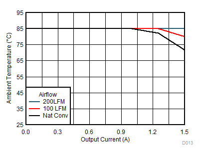
(2) The ambient temperature is the air temperature of the surrounding environment. The junction temperature is the temperature of the internal power IC when the device is powered. Operating below the maximum ambient temperature, as shown in the safe operating area (SOA) curves, ensures that the maximum junction temperature of any component inside the module is never exceeded.
6.2 Recommended Operating Conditions
Over operating free-air temperature range (unless otherwise noted)
| PARAMETER |
MIN |
MAX |
UNIT |
| VIN |
Input voltage |
TPSM84203 |
4.5 |
28 |
V |
| TPSM84205 |
7 |
28 |
V |
| TPSM84212 |
14.5 |
28 |
V |
| IOUT |
Output current |
0 |
1.5 |
A |
| TA |
Operating ambient temperature range(1) |
–40 |
85 |
°C |
| TJ |
Operating junction temperature range(1) |
–40 |
125 |
°C |
(1) The ambient temperature is the air temperature of the surrounding environment. The junction temperature is the temperature of the internal power IC when the device is powered. Operating below the maximum ambient temperature, as shown in the safe operating area (SOA) curves, ensures that the maximum junction temperature of any component inside the module is never exceeded.
6.3 ESD Ratings
|
VALUE |
UNIT |
| V(ESD) |
Electrostatic discharge |
Human-body model (HBM), per ANSI/ESDA/JEDEC JS-001(1) |
±2500 |
V |
| Charged-device model (CDM), per JEDEC specification JESD22-C101(2) |
±1500 |
(1) JEDEC document JEP155 states that 500-V HBM allows safe manufacturing with a standard ESD control process.
(2) JEDEC document JEP157 states that 250-V CDM allows safe manufacturing with a standard ESD control process.
6.4 Thermal Information
| THERMAL METRIC(1) |
TPSM842xx |
UNIT |
| EAB |
| 3 PINS |
| RθJA |
Junction-to-ambient thermal resistance (2) |
56 |
°C/W |
| ψJT |
Junction-to-top characterization parameter (3) |
0.9 |
°C/W |
| ψJB |
Junction-to-board characterization parameter (4) |
1.7 |
°C/W |
(2) The junction-to-ambient thermal resistance, RθJA, applies to devices soldered directly to a 50 mm × 50 mm double-sided PCB with 2 oz. copper and natural convection cooling. Additional airflow reduces RθJA.
(3) The junction-to-top characterization parameter, ψJT, estimates the junction temperature, TJ, of a device in a real system, using a procedure described in JESD51-2A (sections 6 and 7). TJ = ψJT × Pdis + TT; where Pdis is the power dissipated in the device and TT is the temperature of the top of the controller IC.
(4) The junction-to-board characterization parameter, ψJB, estimates the junction temperature, TJ, of a device in a real system, using a procedure described in JESD51-2A (sections 6 and 7). TJ = ψJB × Pdis + TB; where Pdis is the power dissipated in the device and TB is the temperature of the module board 1 mm from the controller IC.
6.5 Electrical Characteristics
Over -40°C to +85°C free-air temperature range, VIN = 24 V, IOUT = IOUT max, FSW = 400 kHz, CIN = 0.1µF, 50V ceramic; 10µF, 50V ceramic; 100µF, 35V electrolytic, and COUT = 2 x 47µF, 16V 1210 ceramic (unless otherwise noted)
| PARAMETER |
TEST CONDITIONS |
MIN |
TYP |
MAX |
UNIT |
| INPUT VOLTAGE (VIN) |
| VIN |
Input voltage range |
Over VOUT range |
TPSM84203 |
4.5(1) |
|
28 |
V |
| TPSM84205 |
7(1) |
|
28 |
V |
| TPSM84212 |
14.5(1) |
|
28 |
V |
| VIN_UVLO |
VIN under voltage lock out |
VIN increasing |
|
4.1 |
4.4 |
V |
| VIN decreasing |
3.3 |
3.6 |
|
V |
| OUTPUT VOLTAGE (VOUT) |
| VOUT |
Output voltage |
Over IOUT range |
TPSM84203 |
|
3.3 |
|
V |
| TPSM84205 |
|
5.0 |
|
V |
| TPSM84212 |
|
12.0 |
|
V |
| Set-point voltage tolerance |
TA = 25°C, IOUT = 0 A |
–3% |
|
+3% |
|
| Temperature variation(2) |
–40°C ≤ TA ≤ 85°C, IOUT = 0 A |
|
0.4% |
|
|
| Line regulation |
Over VIN range, IOUT = 1 A |
|
0.4% |
|
|
| Load regulation |
Over IOUT range |
|
0.5% |
|
|
|
Output voltage ripple |
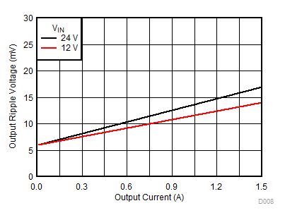
20 MHz bandwidth, peak-to-peak, IOUT > 500 mA |
|
15 |
|
mV |
| OUTPUT CURRENT |
| IOUT |
Output current |
See SOA graph for derating over temperature. |
0 |
|
1.5 |
A |
| Overcurrent threshold |
|
|
3.1 |
|
A |
| PERFORMANCE |
| ƞ |
Efficiency(3) |
VIN = 5 V, IOUT = 1 A |
VOUT = 3.3 V |
|
92% |
|
|
| VIN = 12 V, IOUT = 1 A |
VOUT = 3.3 V |
|
91% |
|
|
| VOUT = 5.0 V |
|
92% |
|
|
| VIN = 24 V, IOUT = 1 A |
VOUT = 3.3 V |
|
87% |
|
|
| VOUT = 5.0 V |
|
90% |
|
|
| VOUT = 12.0 V |
|
94% |
|
|
|
Transient response(2) |
1 A/µs load step,
25% to 75% IOUT(max),
COUT= 94 µF |
VOUT over/undershoot |
|
4% |
|
VOUT |
| Recovery time |
|
100 |
|
µs |
| SOFT START |
| TSS |
Internal soft start time(2) |
|
|
5 |
|
ms |
| THERMAL SHUTDOWN |
|
Rising threshold(2) |
|
|
165 |
|
°C |
|
Hysteresis(2) |
|
|
10 |
|
°C |
| CAPACITANCE |
| CIN |
External input capacitance |
Ceramic type |
10 |
|
|
µF |
| Non-ceramic type |
0 |
100 |
|
µF |
| COUT |
External output capacitance |
Ceramic type |
TPSM84203 |
94 |
|
470 |
µF |
| TPSM84205 |
| TPSM84212 |
47 |
|
470 |
µF |
| Total output capacitance |
0 |
|
500(4) |
µF |
| Equivalent series resistance (ESR) |
|
|
35 |
mΩ |
(1) The minimum input voltage is the lowest ensured voltage that will produce the nominal output voltage. See the
Drop-Out Voltage section for information on drop-out voltage.
(2) Specified by design. Not production tested.
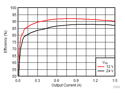
(3) See the efficiency graphs in the Typical Characteristics section for efficiency over the entire load range.
(4) The maximum output capacitance of 500 μF includes the combination of both ceramic and non-ceramic capacitors.
6.6 Switching Characteristics
Over operating free-air temperature range (unless otherwise noted)
| PARAMETER |
TEST CONDITIONS |
MIN |
TYP |
MAX |
UNIT |
| FSW |
Switching frequency |
|
290 |
400 |
510 |
kHz |
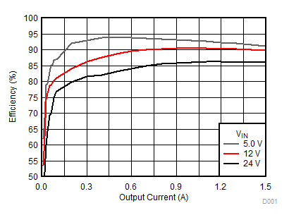
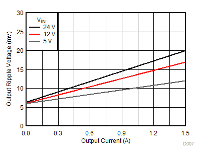
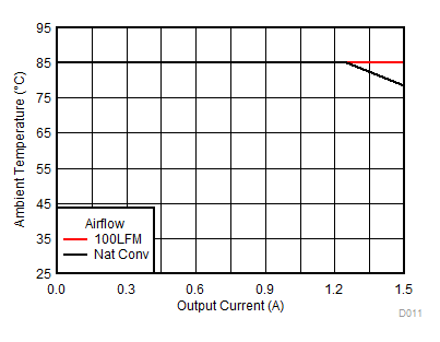
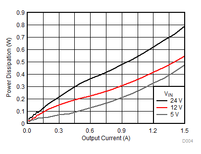
6.7 Typical Characteristics (VOUT = 3.3 V)
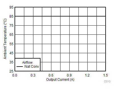
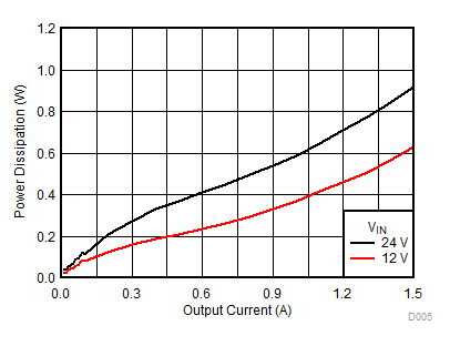
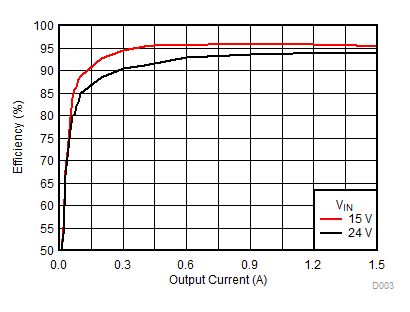
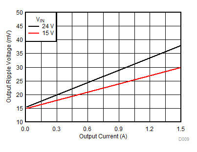
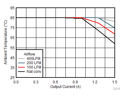
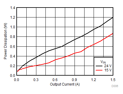
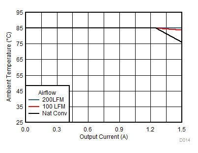
Typical characteristic data has been developed from actual products tested at 25°C. This data is considered typical for the device. Safe operating area curves were measured using a Texas Instruments evaluation module (EVM).
 Figure 1. Efficiency vs Output Current

| VOUT = 3.3 V |
COUT = 2x 47 µF |
|
Figure 3. Ripple Voltage vs Output Current
 Figure 5. Safe Operating Area
 Figure 2. Power Dissipation vs Output Current
 Figure 4. Safe Operating Area
6.8 Typical Characteristics (VOUT = 5 V)
Typical characteristic data has been developed from actual products tested at 25°C. This data is considered typical for the device. Safe operating area curves were measured using a Texas Instruments evaluation module (EVM).
 Figure 6. Efficiency vs Output Current

| VOUT = 5 V |
COUT = 2x 47 µF |
|
Figure 8. Ripple Voltage vs Output Current
 Figure 10. Safe Operating Area
 Figure 7. Power Dissipation vs Output Current
 Figure 9. Safe Operating Area
6.9 Typical Characteristics (VOUT = 12 V)
Typical characteristic data has been developed from actual products tested at 25°C. This data is considered typical for the device. Safe operating area curves were measured using a Texas Instruments evaluation module (EVM).
 Figure 11. Efficiency vs Output Current

| VOUT = 12 V |
COUT = 1x 47 µF |
|
Figure 13. Ripple Voltage vs Output Current
 Figure 15. Safe Operating Area
 Figure 12. Power Dissipation vs Output Current
 Figure 14. Safe Operating Area
