SLWS224E August 2010 – January 2016 TRF372017
PRODUCTION DATA.
- 1 Features
- 2 Applications
- 3 Description
- 4 Revision History
- 5 Pin Configuration and Functions
- 6 Specifications
-
7 Detailed Description
- 7.1 Overview
- 7.2 Functional Block Diagram
- 7.3
Feature Description
- 7.3.1 Integer and Fractional Mode Selection
- 7.3.2 Description of PLL Structure
- 7.3.3 Fractional Mode Setup
- 7.3.4 Selecting the VCO and VCO Frequency Control
- 7.3.5 External VCO
- 7.3.6 VCO Test Mode
- 7.3.7 Lock Detect
- 7.3.8 Tx Divider
- 7.3.9 LO Divider
- 7.3.10 Mixer
- 7.3.11 Disabling Outputs
- 7.3.12 Power Supply Distribution
- 7.3.13 Carrier Feedthrough Cancellation
- 7.3.14 Internal Baseband Bias Voltage Generation
- 7.4 Device Functional Modes
- 7.5 Register Maps
- 8 Application and Implementation
- 9 Power Supply Recommendations
- 10Layout
- 11Device and Documentation Support
- 12Mechanical, Packaging, and Orderable Information
Package Options
Mechanical Data (Package|Pins)
- RGZ|48
Thermal pad, mechanical data (Package|Pins)
- RGZ|48
Orderable Information
8 Application and Implementation
NOTE
Information in the following applications sections is not part of the TI component specification, and TI does not warrant its accuracy or completeness. TI’s customers are responsible for determining suitability of components for their purposes. Customers should validate and test their design implementation to confirm system functionality.
8.1 Application Information
The TRF372017 is suited for quadrature up-conversion applications such as wireless radio transmitters.
8.2 Typical Application
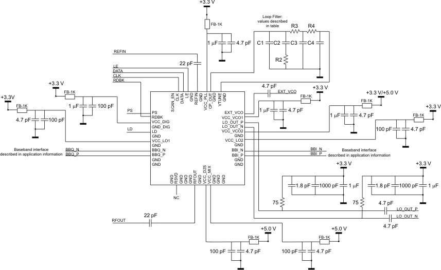
8.2.1 Design Requirements
Table 22 shows the design requirements for this application.
Table 22. Quadrature Up-Converter Design Requirements for Wireless Transmitter Application
| PARAMETER | REQUIREMENT(1) | TRF372017 PERFORMANCE |
|---|---|---|
| Gain | –5 to 0 dB | –3.1 dB |
| Noise figure, NF | <21 dB | 19 dB |
| 3rd order intercept (IIP3) | >+20 dBm | +25 dBm |
| 1dB compression (P1dB) | >+10 dBm | +11.5 dBm |
| ACPR | >70 dBc | 75 dBc |
| RF output frequency range | 1500 to 2500 MHz | 300 to 4300 MHz |
| LO input frequency range | 1000 to 3000 MHz | 300 to 4800 MHz |
| IF input frequency range | DC - 150 MHz | DC - 1 GHz |
| LO phase noise | <–130 dBc/Hz, 1 GHz, 1 MHz offset | –137 dBc/Hz, 1 GHz, 1 MHz offset |
8.2.2 Detailed Design Procedure
8.2.2.1 DAC Interfacing With External Baseband Bias Voltage
Common-mode voltage on the baseband inputs can be generated either internally or externally. An external interface must provide 1.7-V DC and any necessary filtering. A typical interface to a DAC device is shown in Figure 86.
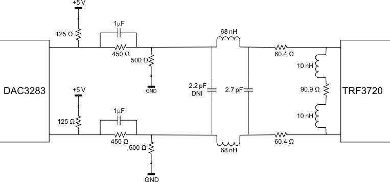 Figure 86. DAC to TRF372017 Interface With External VCM Generation
8.2.2.2 DAC Interface Using Internal VCM Generation
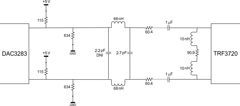
A typical DAC to TRF372017 interface using internal VCM generation is shown in Figure 87.
8.2.2.3 LO Outputs
The LO outputs are open collector outputs. They require a pullup to VCC. 75-Ω pullup resistors to VCC with local decoupling provides a good broadband match and is shown in an example circuit in Figure 88. An inductor pullup in parallel with a cap can provide a tuned load for excellent narrowband load matching.
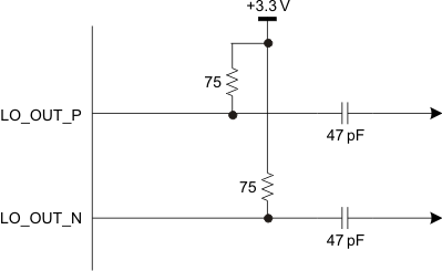 Figure 88. Example LO_OUT Circuit for Broadband Operation
8.2.2.4 Loop Filter
Loop filter design is critical for achieving low closed loop phase noise. Some typical loop filter component values are given in Table 23, referenced to designators in Figure 89. These loop filters are designed using charge pump current of 1.94 mA to minimize noise.
Table 23. Typical Loop Filter Components
| fPFD (MHz) | C1 (pF) | C2 (pF) | R2 (kΩ) | C3 (pF) | R3 (kΩ) | C4 (pF) | R4 (kΩ) |
|---|---|---|---|---|---|---|---|
| 40 | 1000 | 10000 | 0.47 | 39 | 1.4 | 1.8 | 3.3 |
| 1.6 | 47 | 560 | 10 | 4.7 | 5 | open | 0 |
| 6.4 | 100 | 1000 | 5 | 20 | 5 | open | 0 |
| 10 | 270 | 4700 | 1.5 | 4700 | 1.5 | open | 0 |
| 30.72 | 2200 | 20000 | 0.47 | 220 | 0.475 | 220 | 0.475 |
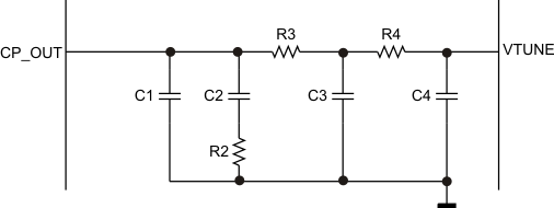 Figure 89. Loop Filter Component Reference Designators
8.2.2.5 ESD Sensitivity
RF devices may be extremely sensitive to electrostatic discharge (ESD) (see ). To prevent damage from electrostatic discharge (ESD), devices must be stored and handled in a way that prevents the build up of electrostatic voltages that exceed the rated level. Rated electrostatic discharge (ESD) levels shall also not be exceeded while the device is installed on a printed-circuit board.
8.2.3 Application Curves
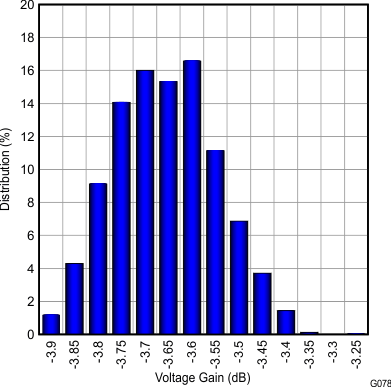 Figure 90. Gain at 2300-MHz Distribution
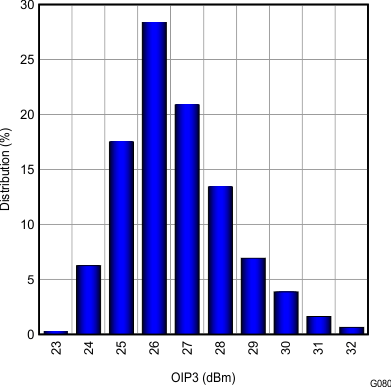 Figure 92. OIP3 at 2300-MHz Distribution
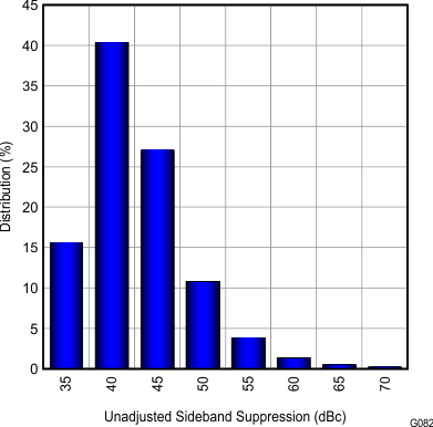 Figure 94. Unadjusted Sideband Suppression
 at 2300-MHz Distribution
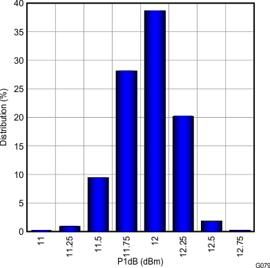 Figure 91. P1dB at 2300-MHz Distribution
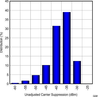 Figure 93. Unadjusted Carrier Suppression
 at 2300-MHz Distribution
