SLASE41 May 2014 TRF37B73
PRODUCTION DATA.
- 1 Features
- 2 Applications
- 3 Description
- 4 Revision History
- 5 Pin Configuration and Functions
- 6 Specifications
- 7 Detailed Description
- 8 Applications and Implementation
- 9 Power Supply Recommendations
- 10Layout
- 11Device and Documentation Support
- 12Mechanical, Packaging, and Orderable Information
Package Options
Mechanical Data (Package|Pins)
- DSG|8
Thermal pad, mechanical data (Package|Pins)
- DSG|8
Orderable Information
5 Pin Configuration and Functions
DSG PACKAGE
(TOP VIEW)
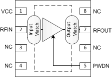
Pin Functions
| PIN | DESCRIPTION | |
|---|---|---|
| NAME | NO. | |
| VCC | 1 | DC Bias. |
| RFIN | 2 | RF input. Connect to an RF source through a DC-blocking capacitor. Internally matched to 50 Ω. |
| NC | 3, 4, 6, 8 | No electrical connection. Connect pad to GND for board level reliability integrity. |
| PWDN | 5 | When high the device is in power down state. When LOW or NC the device is in active state. Internal pulldown resistor to GND. |
| RFOUT | 7 | RF Output and DC Bias (VCC). Connect to DC supply through an RF choke inductor. Connect to output load through a DC-blocking capacitor. Internally matched to 50 Ω. |
| GND | PowerPAD™ | RF and DC GND. Connect to PCB ground plane. |