SLASE42 May 2014 TRF37C73
PRODUCTION DATA.
- 1 Features
- 2 Applications
- 3 Description
- 4 Revision History
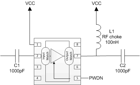
- 5 Pin Configuration and Functions
- 6 Specifications
- 7 Detailed Description
- 8 Applications and Implementation
- 9 Power Supply Recommendations
- 10Layout
- 11Device and Documentation Support
- 12Mechanical, Packaging, and Orderable Information
Package Options
Mechanical Data (Package|Pins)
- DSG|8
Thermal pad, mechanical data (Package|Pins)
- DSG|8
Orderable Information
1 Features
- 1 MHz – 6000 MHz
- Gain: 17 dB
- Noise Figure: 3.5 dB
- Output P1dB: 16.5 dBm at 2000 MHz
- Output IP3: 28.5 dBm at 2000 MHz
- Power Down Mode
- Single Supply: 3.3 V
- Stabilized Performance Over Temperature
- Unconditionally Stable
- Robust ESD: >1 kV HBM; >1 kV CDM
2 Applications
- General Purpose RF Gain Block
- Consumer
- Industrial
- Utility Meters
- Low-cost Radios
- Cellular Base Station
- Wireless Infrastructure
- RF Backhaul
- Radar
- Electronic Warfare
- Software-defined Radio
- Test and Measurement
- Point-to-Point/Multipoint Microwave
- Software Defined Radios
- RF Repeaters
- Distributed Antenna Systems
- LO and PA Driver Amplifier
- Wireless Data, Satellite, DBS, CATV
- IF Amplifier
3 Description
The TRF37C73 is packaged in a 2.00mm x 2.00mm WSON with a power down pin feature making it ideal for applications where space and low power modes are critical.
The TRF37C73 is designed for ease of use. For maximum flexibility, this family of parts uses a common 3.3 V supply and consumes 55 mA. In addition, this family was designed with an active bias circuit that provides a stable and predictable bias current over process, temperature and voltage variations. For gain and linearity budgets the device was designed to provide a flat gain response and excellent OIP3 out to 6000 MHz. For space constrained applications, this family is internally matched to 50 Ω, which simplifies ease of use and minimizes needed PCB area.
Device Information(1)
| PART NUMBER | PACKAGE | BODY SIZE (NOM) |
|---|---|---|
| TRF37C73 | WSON (32) | 2.00mm x 2.00mm |
- For all available packages, see the orderable addendum at the end of the datasheet.
Simplified Schematic