SLOS743M August 2011 – March 2020 TRF7970A
PRODUCTION DATA.
- 1Device Overview
- 2Revision History
- 3Device Characteristics
- 4Terminal Configuration and Functions
- 5Specifications
-
6Detailed Description
- 6.1 Overview
- 6.2 System Block Diagram
- 6.3 Power Supplies
- 6.4 Receiver – Analog Section
- 6.5 Receiver – Digital Section
- 6.6 Oscillator Section
- 6.7 Transmitter – Analog Section
- 6.8 Transmitter – Digital Section
- 6.9 Transmitter – External Power Amplifier and Subcarrier Detector
- 6.10 TRF7970A IC Communication Interface
- 6.11 TRF7970A Initialization
- 6.12 Special Direct Mode for Improved MIFARE Compatibility
- 6.13 NFC Modes
- 6.14
Direct Commands from MCU to Reader
- 6.14.1
Command Codes
- 6.14.1.1 Idle (0x00)
- 6.14.1.2 Software Initialization (0x03)
- 6.14.1.3 Initial RF Collision Avoidance (0x04)
- 6.14.1.4 Response RF Collision Avoidance (0x05)
- 6.14.1.5 Response RF Collision Avoidance (0x06, n = 0)
- 6.14.1.6 Reset FIFO (0x0F)
- 6.14.1.7 Transmission With CRC (0x11)
- 6.14.1.8 Transmission Without CRC (0x10)
- 6.14.1.9 Delayed Transmission With CRC (0x13)
- 6.14.1.10 Delayed Transmission Without CRC (0x12)
- 6.14.1.11 Transmit Next Time Slot (0x14)
- 6.14.1.12 Block Receiver (0x16)
- 6.14.1.13 Enable Receiver (0x17)
- 6.14.1.14 Test Internal RF (RSSI at RX Input With TX ON) (0x18)
- 6.14.1.15 Test External RF (RSSI at RX Input with TX OFF) (0x19)
- 6.14.1
Command Codes
- 6.15
Register Description
- 6.15.1 Register Preset
- 6.15.2 Register Overview
- 6.15.3
Detailed Register Description
- 6.15.3.1 Main Configuration Registers
- 6.15.3.2
Control Registers – Sublevel Configuration Registers
- 6.15.3.2.1 ISO/IEC 14443 TX Options Register (0x02)
- 6.15.3.2.2 ISO/IEC 14443 High-Bit-Rate and Parity Options Register (0x03)
- 6.15.3.2.3 TX Timer High Byte Control Register (0x04)
- 6.15.3.2.4 TX Timer Low Byte Control Register (0x05)
- 6.15.3.2.5 TX Pulse Length Control Register (0x06)
- 6.15.3.2.6 RX No Response Wait Time Register (0x07)
- 6.15.3.2.7 RX Wait Time Register (0x08)
- 6.15.3.2.8 Modulator and SYS_CLK Control Register (0x09)
- 6.15.3.2.9 RX Special Setting Register (0x0A)
- 6.15.3.2.10 Regulator and I/O Control Register (0x0B)
- 6.15.3.3
Status Registers
- 6.15.3.3.1 IRQ Status Register (0x0C)
- 6.15.3.3.2 Interrupt Mask Register (0x0D) and Collision Position Register (0x0E)
- 6.15.3.3.3 RSSI Levels and Oscillator Status Register (0x0F)
- 6.15.3.3.4 Special Functions Register (0x10)
- 6.15.3.3.5 Special Functions Register (0x11)
- 6.15.3.3.6 Adjustable FIFO IRQ Levels Register (0x14)
- 6.15.3.3.7 NFC Low Field Level Register (0x16)
- 6.15.3.3.8 NFCID1 Number Register (0x17)
- 6.15.3.3.9 NFC Target Detection Level Register (0x18)
- 6.15.3.3.10 NFC Target Protocol Register (0x19)
- 6.15.3.4 Test Registers
- 6.15.3.5 FIFO Control Registers
- 7Applications, Implementation, and Layout
- 8Device and Documentation Support
- 9Mechanical, Packaging, and Orderable Information
Package Options
Mechanical Data (Package|Pins)
- RHB|32
Thermal pad, mechanical data (Package|Pins)
- RHB|32
Orderable Information
6.10.6 Direct Mode
Direct mode allows the user to configure the reader in one of two ways. Direct mode 0 (bit 6 = 0, as defined in ISO Control register) allows the user to use only the front-end functions of the reader, bypassing the protocol implementation in the reader. For transmit functions, the user has direct access to the transmit modulator through the MOD pin (pin 14). On the receive side, the user has direct access to the subcarrier signal (digitized RF envelope signal) on I/O_6 (pin 23).
Direct mode 1 (bit 6 = 1, as defined in ISO Control register) uses the subcarrier signal decoder of the selected protocol (as defined in ISO Control register). This means that the receive output is not the subcarrier signal but the decoded serial bit stream and bit clock signals. The serial data is available on I/O_6 (pin 23) and the bit clock is available on I/O_5 (pin 22). The transmit side is identical; the user has direct control over the RF modulation through the MOD input. This mode is provided so that the user can implement a protocol that has the same bit coding as one of the protocols implemented in the reader, but needs a different framing format.
To select direct mode, the user must first choose which direct mode to enter by writing B6 in the ISO Control register. This bit determines if the receive output is the direct subcarrier signal (B6 = 0) or the serial data of the selected decoder. If B6 = 1, then the user must also define which protocol should be used for bit decoding by writing the appropriate setting in the ISO Control register.
The reader actually enters the direct mode when B6 (direct) is set to 1 in the chip status control register. Direct mode starts immediately. The write command should not be terminated with a stop condition (see communication protocol), because the stop condition terminates the direct mode and clears B6. This is necessary as the direct mode uses one or two I/O pins (I/O_6, I/O_5). Normal parallel communication is not possible in direct mode. Sending a stop condition terminates direct mode.
NOTE
An additional direct mode known as special direct mode can be used to communicate with certain tags not compliant with ISO standards. For full details on how to use this feature, see Using Special Direct Mode With the TRF7970A.
Figure 6-27 shows the different configurations available in direct mode.
- In mode 0, the reader is used as an AFE only, and protocol handling is bypassed.
- In mode 1, framing is not done, but SOF and EOF are present. This allows for a user-selectable framing level based on an existing ISO standard.
- In mode 2, data is ISO-standard formatted. SOF, EOF, and error checking are removed, so the microprocessor receives only bytes of raw data through a 127-byte FIFO.
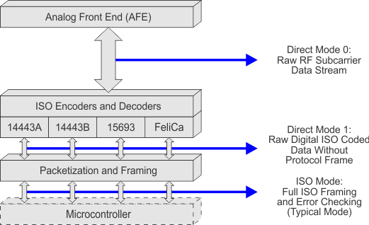 Figure 6-27 User-Configurable Modes
 The steps to enter direct mode are listed below, using SPI with SS communication method only as one example, as direct modes are also possible with parallel and SPI without SS. The must enter direct mode 0 to accommodate card type communications that are not compliant with ISO standards. Direct mode can be entered at any time, so if a card type started with ISO standard communications, then deviated from the standard after being identified and selected, the ability to go into direct mode 0 is very useful.
Step 1: Configure Pins I/O_0 to I/O_2 for SPI with SS
Step 2: Set Pin 12 of the TRF7970A (ASK/OOK pin) to 0 for ASK or 1 for OOK
Step 3: Program the TRF7970A registers
The following registers must be explicitly set before going into the direct mode.
- ISO Control register (0x01) to the appropriate standard
- Modulator and SYS_CLK register (0x09) to the appropriate clock speed and modulation
- 0x21 for 6.78 MHz Clock and OOK (100%) modulation
- 0x20 for 6.78 MHz Clock and ASK 10% modulation
- 0x22 for 6.78 MHz Clock and ASK 7% modulation
- 0x23 for 6.78 MHz Clock and ASK 8.5% modulation
- 0x24 for 6.78 MHz Clock and ASK 13% modulation
- 0x25 for 6.78 MHz Clock and ASK 16% modulation
(See register 0x09 definition for all other possible values)
Example register setting for ISO/IEC 14443 A at 106 kbps:
- ISO Control register (0x01) to 0x08
- RX No Response Wait Time register (0x07) to 0x0E
- RX Wait Time register (0x08) to 0x07
- Modulator control register (0x09) to 0x21 (or any custom modulation)
- RX Special Settings register (0x0A) to 0x20
Step 4: Entering Direct Mode 0
The following registers must be programmed to enter direct mode 0:
- Set bit B6 of the Modulator and SYS_CLK Control register (0x09) to 1.
- Set bit B6 of the ISO Control (Register 01) to 0 for direct mode 0 (default its 0)
- Set bit B6 of the Chip Status Control register (0x00) to 1 to enter direct mode
- Send extra eight clock cycles (see Figure 6-28, this step is TRF7970A specific)
- It is important that the last write is not terminated with a stop condition. For SPI, this means that Slave Select (I/O_4) stays low.
- Sending a Stop condition terminates the direct mode and clears bit B6 in the Chip Status Control register (0x00).
NOTE
NOTE
Access to Registers, FIFO, and IRQ is not available during direct mode 0.
The reader enters the direct mode 0 when bit 6 of the Chip Status Control register (0x00) is set to a 1 and stays in direct mode 0 until a stop condition is sent from the microcontroller.
NOTE
The write command should not be terminated with a stop condition (for example, in SPI mode this is done by bringing the Slave Select line high after the register write), because the stop condition terminates the direct mode and clears bit 6 of the Chip Status Control register (0x00), making it a 0.
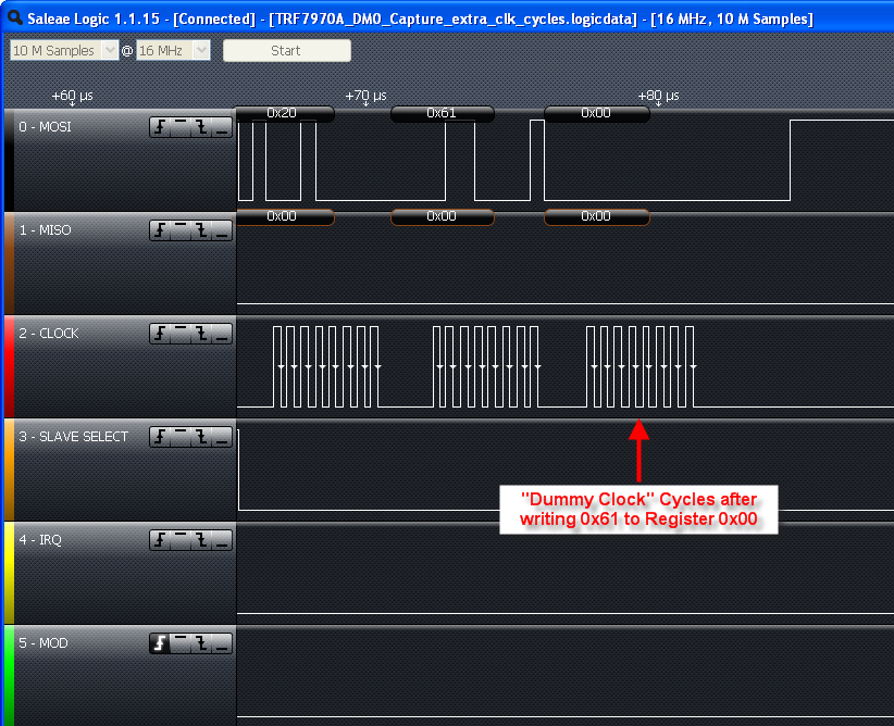 Figure 6-28 Entering Direct Mode 0
 Step 5: Transmit Data Using Direct Mode
The application now has direct control over the RF modulation through the MOD input (see Figure 6-29).
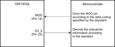 Figure 6-29 Direct Control Signals
 The microcontroller is responsible for generating data according to the coding specified by the particular standard. The microcontroller must generate SOF, EOF, Data, and CRC. In direct mode, the FIFO is not used and no IRQs are generated. See the applicable ISO standard to understand bit and frame definitions. Figure 6-30 shows an example of what the developer sees when using DM0 in an actual application. This figure clearly shows the relationship between the MOD pin being controlled by the MCU and the resulting modulated 13.56-MHz carrier signal.
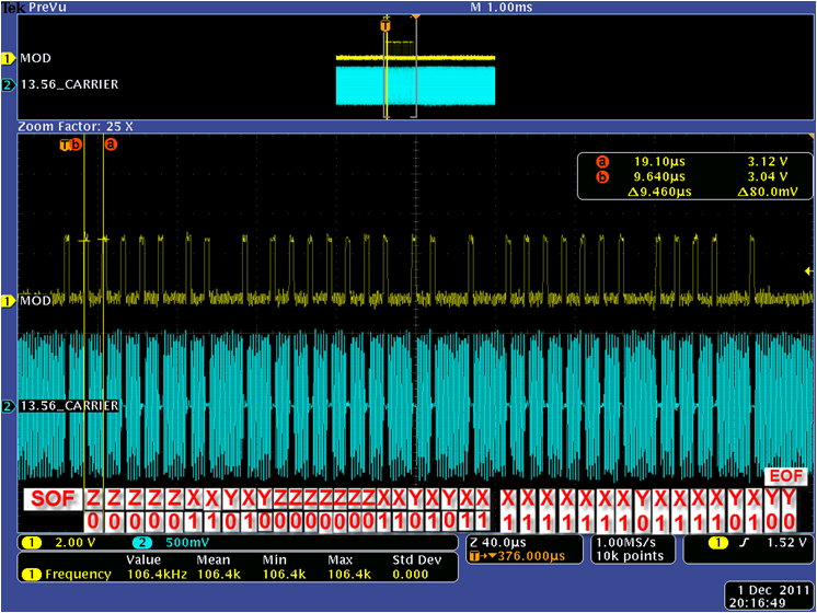 Figure 6-30 TX Sequence Out in DM0
 Step 6: Receive Data Using Direct Mode
After the TX operation is complete, the tag responds to the request and the subcarrier data is available on pin I/O_6. The microcontroller needs to decode the subcarrier signal according to the standard. This includes decoding the SOF, data bits, CRC, and EOF. The CRC then needs to be checked to verify data integrity. The receive data bytes must be buffered locally.
As an example of the receive data bits and framing level according to the ISO/IEC 14443 A standard is shown in Figure 6-31 (taken from ISO/IEC 14443 specification and TRF7970A air interface).
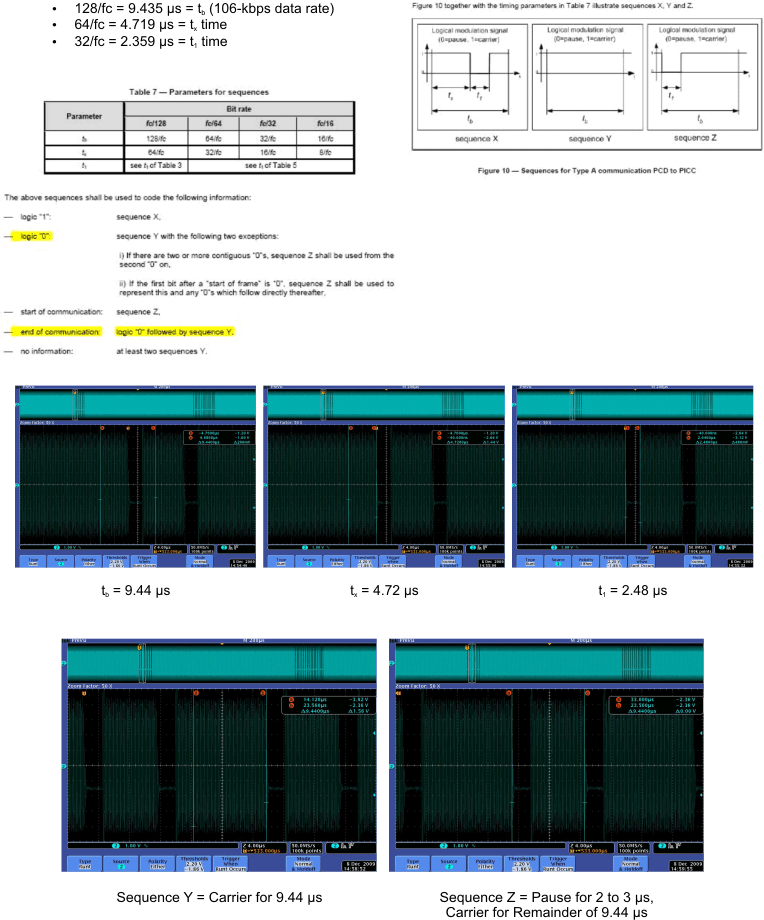 Figure 6-31 Receive Data Bits and Framing Level
 Figure 6-32 shows an example of what the developer should expect on the I/O_6 line during the RX process while in direct mode 0.
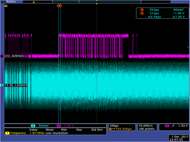 Figure 6-32 RX Sequence on I/O_6 in DM0 (Analog Capture)
 Step 7: Terminating Direct Mode 0
After the EOF is received, data transmission is over, and direct mode 0 can be terminated by sending a Stop Condition (in the case of SPI, make the Slave Select go high). The TRF7970A is returned to default state.