SLOS743M August 2011 – March 2020 TRF7970A
PRODUCTION DATA.
- 1Device Overview
- 2Revision History
- 3Device Characteristics
- 4Terminal Configuration and Functions
- 5Specifications
-
6Detailed Description
- 6.1 Overview
- 6.2 System Block Diagram
- 6.3 Power Supplies
- 6.4 Receiver – Analog Section
- 6.5 Receiver – Digital Section
- 6.6 Oscillator Section
- 6.7 Transmitter – Analog Section
- 6.8 Transmitter – Digital Section
- 6.9 Transmitter – External Power Amplifier and Subcarrier Detector
- 6.10 TRF7970A IC Communication Interface
- 6.11 TRF7970A Initialization
- 6.12 Special Direct Mode for Improved MIFARE Compatibility
- 6.13 NFC Modes
- 6.14
Direct Commands from MCU to Reader
- 6.14.1
Command Codes
- 6.14.1.1 Idle (0x00)
- 6.14.1.2 Software Initialization (0x03)
- 6.14.1.3 Initial RF Collision Avoidance (0x04)
- 6.14.1.4 Response RF Collision Avoidance (0x05)
- 6.14.1.5 Response RF Collision Avoidance (0x06, n = 0)
- 6.14.1.6 Reset FIFO (0x0F)
- 6.14.1.7 Transmission With CRC (0x11)
- 6.14.1.8 Transmission Without CRC (0x10)
- 6.14.1.9 Delayed Transmission With CRC (0x13)
- 6.14.1.10 Delayed Transmission Without CRC (0x12)
- 6.14.1.11 Transmit Next Time Slot (0x14)
- 6.14.1.12 Block Receiver (0x16)
- 6.14.1.13 Enable Receiver (0x17)
- 6.14.1.14 Test Internal RF (RSSI at RX Input With TX ON) (0x18)
- 6.14.1.15 Test External RF (RSSI at RX Input with TX OFF) (0x19)
- 6.14.1
Command Codes
- 6.15
Register Description
- 6.15.1 Register Preset
- 6.15.2 Register Overview
- 6.15.3
Detailed Register Description
- 6.15.3.1 Main Configuration Registers
- 6.15.3.2
Control Registers – Sublevel Configuration Registers
- 6.15.3.2.1 ISO/IEC 14443 TX Options Register (0x02)
- 6.15.3.2.2 ISO/IEC 14443 High-Bit-Rate and Parity Options Register (0x03)
- 6.15.3.2.3 TX Timer High Byte Control Register (0x04)
- 6.15.3.2.4 TX Timer Low Byte Control Register (0x05)
- 6.15.3.2.5 TX Pulse Length Control Register (0x06)
- 6.15.3.2.6 RX No Response Wait Time Register (0x07)
- 6.15.3.2.7 RX Wait Time Register (0x08)
- 6.15.3.2.8 Modulator and SYS_CLK Control Register (0x09)
- 6.15.3.2.9 RX Special Setting Register (0x0A)
- 6.15.3.2.10 Regulator and I/O Control Register (0x0B)
- 6.15.3.3
Status Registers
- 6.15.3.3.1 IRQ Status Register (0x0C)
- 6.15.3.3.2 Interrupt Mask Register (0x0D) and Collision Position Register (0x0E)
- 6.15.3.3.3 RSSI Levels and Oscillator Status Register (0x0F)
- 6.15.3.3.4 Special Functions Register (0x10)
- 6.15.3.3.5 Special Functions Register (0x11)
- 6.15.3.3.6 Adjustable FIFO IRQ Levels Register (0x14)
- 6.15.3.3.7 NFC Low Field Level Register (0x16)
- 6.15.3.3.8 NFCID1 Number Register (0x17)
- 6.15.3.3.9 NFC Target Detection Level Register (0x18)
- 6.15.3.3.10 NFC Target Protocol Register (0x19)
- 6.15.3.4 Test Registers
- 6.15.3.5 FIFO Control Registers
- 7Applications, Implementation, and Layout
- 8Device and Documentation Support
- 9Mechanical, Packaging, and Orderable Information
Package Options
Mechanical Data (Package|Pins)
- RHB|32
Thermal pad, mechanical data (Package|Pins)
- RHB|32
Orderable Information
6.10.5.1 Serial Interface Mode With Slave Select (SS)
The serial interface is in reset while the Slave Select signal is high. Serial data in (MOSI) changes on the rising edge, and is validated in the reader on the falling edge, as shown in Figure 6-19. Communication is terminated when the Slave Select signal goes high.
All words must be 8 bits long with the MSB transmitted first.
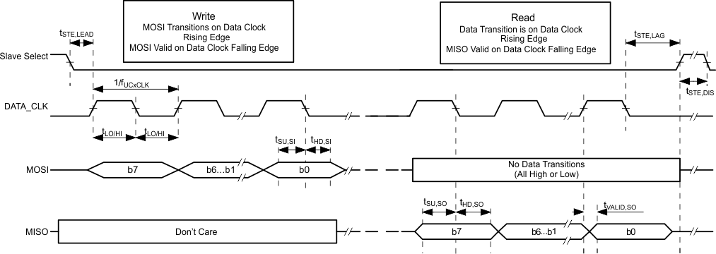 Figure 6-19 SPI With Slave Select Timing Diagram
 The read command is sent out on the MOSI pin, MSB first, in the first eight clock cycles. MOSI data changes on the rising edge, and is validated in the reader on the falling edge, as shown in Figure 6-19. During the write cycle, the serial data out (MISO) is not valid. After the last read command bit (B0) is validated at the eighth falling edge of SCLK, valid data can be read on the MISO pin at the falling edge of SCLK. It takes eight clock edges to read out the full byte (MSB first). See Section 5.4 for electrical specifications related to Figure 6-19.
Figure 6-20 and Figure 6-21 show the continuous read operation.
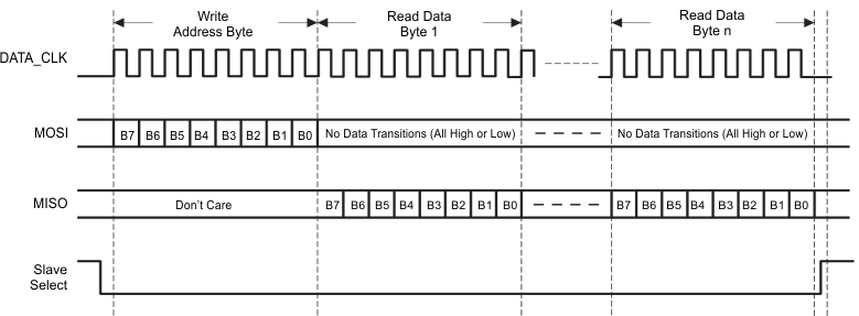 Figure 6-20 Continuous Read Operation Using SPI With Slave Select
 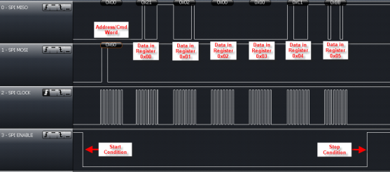 Figure 6-21 Continuous Read of Registers 0x00 to 0x05 Using SPI With SS
 Figure 6-22 shows an example of performing a single slot inventory command. Reader registers (in this example) are configured for 5 VDC in and default operation.
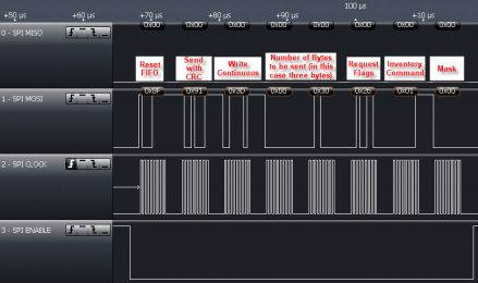 Figure 6-22 Inventory Command Sent From MCU to TRF7970A
 The TRF7970A takes these bytes from the MCU and then send out Request Flags, Inventory Command, and Mask over the air to the ISO/IEC 15693 transponder. After these three bytes have been transmitted, an interrupt occurs to indicate back to the reader that the transmission has been completed. In the example in Figure 6-23, this IRQ occurs approximately 1.6 ms after the SS line goes high after the Inventory command is sent out.
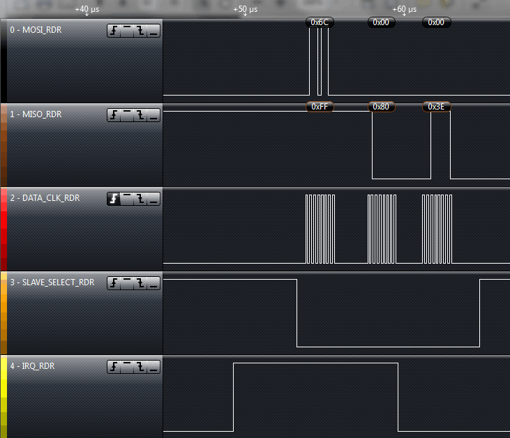
The IRQ status register read (0x6C) yields 0x80, which indicates that TX is indeed complete. This is followed by a dummy clock. Then, if a tag is in the field and no error is detected by the reader, a second interrupt is expected and occurs (in this example) approximately 4 ms after first IRQ is read and cleared.
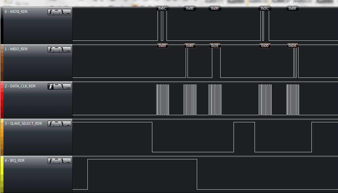
In the continuation of the example (see Figure 6-24), the IRQ Status Register is read using method previously recommended, followed by a single read of the FIFO Status register, which indicates that there are 10 bytes to be read out.
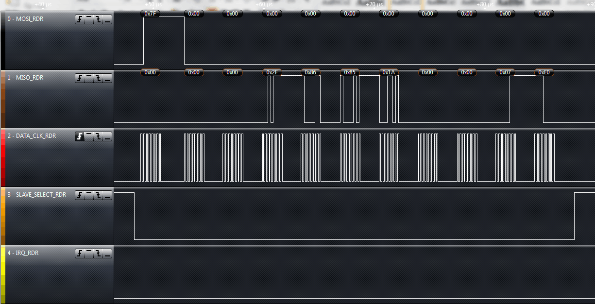
This is then followed by a continuous read of the FIFO (see Figure 6-25). The first byte is (and should be) 0x00 for no error. The next byte is the DSFID (usually shipped by manufacturer as 0x00), then the UID, shown here up to the next most significant byte, the MFG code [shown as 0x07 (TI silicon)].
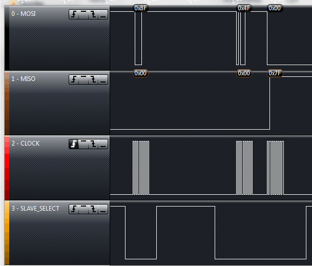
TI recommends resetting the FIFO after receiving data. Additionally, the RSSI value of the tag can be read out at this point. In the example in Figure 6-26, the transponder is very close to the antenna, so value of 0x7F is recovered.
