SLLSET7C May 2016 – May 2016 TRS3122E
PRODUCTION DATA.
- 1 Features
- 2 Applications
- 3 Description
- 4 Revision History
- 5 Pin Configuration and Functions
-
6 Specifications
- 6.1 Absolute Maximum Ratings
- 6.2 ESD Ratings
- 6.3 Recommended Operating Conditions
- 6.4 Thermal Characteristics
- 6.5 Power and Status Electrical Characteristics
- 6.6 Driver Electrical Characteristics
- 6.7 Receiver Electrical Characteristics
- 6.8 Driver Switching Characteristics
- 6.9 Receiver Switching Characteristics
- 6.10 Power and Status Switching Characteristics
- 6.11 Typical Characteristics
- 7 Parameter Measurement Information
- 8 Detailed Description
- 9 Application and Implementation
- 10Power Supply Recommendations
- 11Layout
- 12Device and Documentation Support
- 13Mechanical, Packaging, and Orderable Information
Package Options
Mechanical Data (Package|Pins)
- RGE|24
Thermal pad, mechanical data (Package|Pins)
- RGE|24
Orderable Information
6 Specifications
6.1 Absolute Maximum Ratings(1)
over operating free-air temperature range (unless otherwise noted)| MIN | MAX | UNIT | |||
|---|---|---|---|---|---|
| VCC | Charge pump power supply | –0.3 | 6 | V | |
| VL | Logic power supply | –0.3 | 6 | V | |
| V+ | Positive storage capacitor voltage | –0.3 | 7 | V | |
| V– | Negative storage capacitor voltage | 0.3 | –7 | V | |
| V+ + |V–|(2) | 13 | V | |||
| VI | Input voltage | FORCEOFF , FORCEON | –0.3 | 6 | V |
| DIN | –0.3 | VL + 0.3 | |||
| RIN (0Ω series resistance) | ±20 | ||||
| RIN (≥250Ω series resistance) | ±25 | ||||
| VO | Output voltage | DOUT | ±13.2 | V | |
| ROUT | –0.3 | VL + 0.3 | |||
| TJ | Junction temperature | 150 | °C | ||
| Tstg | Storage temperature range | –65 | 150 | °C | |
(1) Stresses beyond those listed under “absolute maximum ratings” may cause permanent damage to the device. These are stress ratings only, and functional operation of the device at these or any other conditions beyond those indicated in the operational sections of the specifications is not implied. Exposure to absolute maximum rating conditions for extended periods may affect device reliability.
(2) V+ and V– can have maximum magnitudes of 7 V, but their absolute difference cannot exceed 13 V.
6.2 ESD Ratings
| VALUE | UNIT | ||||
|---|---|---|---|---|---|
| V(ESD) | Electrostatic discharge | Human body model (HBM), per ANSI/ESDA/JEDEC JS-001, all pins(1) | All pins except RS-232 bus | ±2000 | V |
| RS-232 bus pins | ±15000 | ||||
| Charged device model (CDM), per JEDEC specification JESD22-C101, all pins(2) | All pins | ±500 | |||
| IEC 61000-4-2 Air-Gap Discharge | RS-232 bus pins | ±15000 | |||
| IEC 61000-4-2 Contact Discharge | ±8000 | ||||
(1) JEDEC document JEP155 states that 500-V HBM allows safe manufacturing with a standard ESD control process.
(2) JEDEC document JEP157 states that 250-V CDM allows safe manufacturing with a standard ESD control process.
6.3 Recommended Operating Conditions
| MIN | TYP | MAX | UNIT | ||||
|---|---|---|---|---|---|---|---|
| VCC | Charge pump power supply | Tripler Mode | 1.65 | 1.8 | 2 | V | |
| Doubler Mode | 3 | 3.3 | 3.6 | ||||
| 4.5 | 5 | 5.5 | |||||
| VL | Logic power supply | 1.65 | VCC | V | |||
| RIN | RS-232 Receiver interface | -15 | 15 | V | |||
| DOUT | RS-232 Transmitter interface | -12 | 12 | V | |||
| VIL | GPIO Input logic threshold low | DIN, FORCEOFF, FORCEON | VL = 5.0 V | 0 | 1.7 | V | |
| VL = 3.3V | 0 | 1.1 | |||||
| VL = 1.8 V | 0 | 0.6 | |||||
| VIH | GPIO Input logic threshold high | DIN, FORCEOFF, FORCEON | VL = 5.0V | 3.3 | VL | V | |
| VL = 3.3V | 2.2 | VL | |||||
| VL = 1.8V | 1.2 | VL | |||||
| VOZ | ROUT disabled | FORCEOFF = 0V | 0 | VL | V | ||
| Operating temperature | –40 | 85 | °C | ||||
6.4 Thermal Characteristics
| THERMAL METRIC | TRS3122E | UNIT | ||
|---|---|---|---|---|
| RGE | ||||
| RθJA | Junction-to-ambient thermal resistance | 34.2 | °C/W | |
| RθJCtop | Junction-to-case (top) thermal resistance | 27.2 | ||
| RθJB | Junction-to-board thermal resistance | 11.4 | ||
| ψJT | Junction-to-top characterization parameter | 0.4 | ||
| ψJB | Junction-to-board characterization parameter | 11.4 | ||
| RθJC(bot) | Junction-to-case (bottom) thermal resistance | 3.6 | ||
6.5 Power and Status Electrical Characteristics
VCC = VL = (1.65 V to 2.0 V) & (3.0V to 5.5V), TA = -40°C to 85°C (unless otherwise noted). Typical data is TA = 25°C, VCC = VL = 3.3V unless otherwise noted.| PARAMETER | TEST CONDITIONS | MIN | TYP | MAX | UNIT | ||||
|---|---|---|---|---|---|---|---|---|---|
| Icc (Static) | DIN1 = GND or VL; DIN2 = GND or VL, FORCEOFF = VL FORCEON = VL | No load | VCC= 1.65V to 2.0V | 1.0 | 1.9 | mA | |||
| VCC= 3.0V to 3.6V | 0.7 | 1.4 | |||||||
| VCC= 4.5V to 5.5V | 0.8 | 1.9 | |||||||
| Icc (off) | FORCEOFF = GND | 0.4 | 10 | μA | |||||
| VIT+ | RIN postive voltage threshold for INVALID output change | RIN1 = RIN2 | 0.3 | 2.4 | V | ||||
| VIT- | RIN negative voltage threshold for INVALID output change | -2.4 | -0.3 | ||||||
| VOH | INVALID high-level output voltage | IOH = -1 mA, FORCEON = GND, FORCEOFF = VL | VL-0.4 | VL-0.08 | VL | V | |||
| VOL | INVALID low-level output voltage | IOL = 1.6 mA, FORCEON = GND, FORCEOFF = VL | 0 | 0.06 | 0.4 | V | |||
6.6 Driver Electrical Characteristics
VCC = VL = (1.65 V to 2.0 V) & (3.0V to 5.5V), TA = -40°C to 85°C (unless otherwise noted). Typical data is TA = 25°C, VCC = VL = 3.3V unless otherwise noted.| PARAMETER | TEST CONDITIONS | MIN | TYP | MAX | UNIT | ||
|---|---|---|---|---|---|---|---|
| VOUT | Output voltage swing | All driver outputs loaded with 3 kΩ to ground C3 = 100 nF, VCC= 1.8 V |
±4.25 | ±4.7 | V | ||
| All driver outputs loaded with 3 kΩ to ground C3 = 0 F, VCC= 3.3 V or 5 V |
±5 | ±5.4 | |||||
| rO | Output resistance | (VCC = V+ = V– = 0); Driver output = ±2 V | 300 | 10M | Ω | ||
| IOS | Output short-circuit current | VDOUT = 0 | ±60 | mA | |||
| IOZ | Output leakage current | VDOUT = ±12 V, FORCEOFF = GND | 0 | ±25 | μA | ||
| Driver input hysteresis | 0.5 | 1 | V | ||||
| Input leakage current | DIN = GND to VL; FORCEOFF = GND to VL; FORCEON = GND to VL | 0 | ±5 | μA | |||
6.7 Receiver Electrical Characteristics
VCC = VL = (1.65 V to 2.0 V) & (3.0V to 5.5V), TA = -40°C to 85°C (unless otherwise noted). Typical data is TA = 25°C, VCC = VL = 3.3V unless otherwise noted.| PARAMETER | TEST CONDITIONS | MIN | TYP | MAX | UNIT | ||
|---|---|---|---|---|---|---|---|
| Ioff | Output leakage current | ROUT, receivers disabled | ±0.01 | ±10 | μA | ||
| VOL | Output voltage low | IOUT= 2.0 mA | 0.04 | 0.3 | V | ||
| VOH | Output voltage high | IOUT= –2.0mA | VL–0.3 | VL–0.04 | V | ||
| VIT– | Input threshold low | TA=25°C | VL= 5 V | 0.8 | 1.5 | V | |
| VL= 3.3 V | 0.7 | 1.1 | |||||
| VL= 1.8 V | 0.6 | 0.7 | |||||
| VIT+ | Input threshold high | TA =25°C | VL= 5 V | 2.0 | 2.4 | V | |
| VL = 3.3 V | 1.5 | 2.4 | |||||
| VL= 1.8 V | 0.9 | 1.4 | |||||
| Vhys | Input hysteresis | TA=25°C | VL= 5 V | 0.45 | V | ||
| VL = 3.3 V | 0.35 | ||||||
| VL= 1.8 V | 0.26 | ||||||
| Input resistance | TA=-40 to 85°C | 3 | 5 | 7 | kΩ | ||
6.8 Driver Switching Characteristics
VCC = VL = (1.65 V to 2.0 V) & (3.0V to 5.5V), TA = -40°C to 85°C (unless otherwise noted). Typical data is TA = 25°C, VCC = VL = 3.3V unless otherwise noted.| PARAMETER | MIN | TYP | MAX | UNIT | |||
|---|---|---|---|---|---|---|---|
| Maximum data rate | RL = 3 kΩ, CL = 500 pF (one driver) | 1000 | kbps | ||||
| RL = 3 kΩ, CL = 1000 pF (one driver) | 500 | ||||||
| Time-to-exit powerdown | |VDOUT| > 3.7 V | 30 | 150 | μs | |||
| |tPHL – tPLH| | Driver skew(1) | RL = 3 kΩ | 0 | 50 | 100 | ns | |
| Transition-region slew rate | RL = 3 kΩ to 7 kΩ, TA = 25°C Measured from 3 V to –3 V or –3 V to 3 V |
VCC = 1.8V, CL = 200 pF | 33 | V/μs | |||
| VCC = 1.8V, CL = 1000 pF | 25 | ||||||
| VCC = 3.3 V, CL = 200 pF | 38 | ||||||
| VCC = 3.3 V, CL = 1000 pF | 28 | ||||||
| VCC = 5 V, CL = 200 pF | 41 | ||||||
| VCC = 5 V, CL = 1000 pF | 30 | ||||||
(1) Driver skew is measured at the driver zero crosspoint.
6.9 Receiver Switching Characteristics
VCC = VL = (1.65 V to 2.0 V) & (3.0V to 5.5V), TA = -40°C to 85°C (unless otherwise noted). Typical data is TA = 25°C, VCC = VL = 3.3V unless otherwise noted.| PARAMETER | TEST CONDITIONS | MIN | TYP | MAX | UNIT | |
|---|---|---|---|---|---|---|
| tPHL | Receiver propagation delay, high to low | Receiver input to receiver output CL = 150 pF |
0.15 | 0.4 | μs | |
| tPLH | Receiver propagation delay, low to high | 0.15 | 0.4 | |||
| tPHL – tPLH | Receiver skew | 50 | 300 | ns | ||
| ten | Receiver output enable time | From FORCEOFF to ROUT= VL/2 CL = 150 pF, RL = 3 kΩ |
200 | 400 | ns | |
| tdis | Receiver output disable time | 200 | 400 | ns | ||
6.10 Power and Status Switching Characteristics
VCC = VL = (1.65 V to 2.0 V) & (3.0V to 5.5V), TA = -40°C to 85°C (unless otherwise noted). Typical data is TA = 25°C, VCC = VL = 3.3V unless otherwise noted.| PARAMETER | MIN | TYP | MAX | UNIT | |
|---|---|---|---|---|---|
| tvalid | Propagation delay time, low- to high-level output | 1 | μs | ||
| tinvalid | Propagation delay time, high- to low-level output | 30 | μs | ||
| tdis | Receiver or driver edge to auto-powerdown plus | 15 | 30 | 60 | s |
6.11 Typical Characteristics
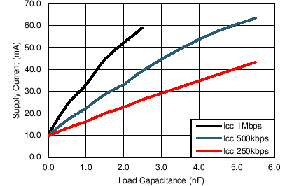 Figure 1. Supply Current vs. Load Capacitance
VCC = 3.3 V, VL = 1.8 V, RLOAD = 3 kΩ, CH2 = 32 kbps
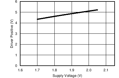 Figure 3. Driver Positive vs. Supply Voltage (Tripler Mode)
1 Mbps, RLOAD = 3 kΩ, CLOAD = 560 pF
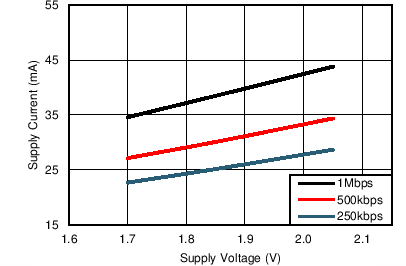 Figure 5. Supply Current vs. Supply Voltage (Tripler Mode)
VL = 1.8 V, RLOAD = 3 kΩ, CLOAD = 1 nF, CH2 = 32 kbps
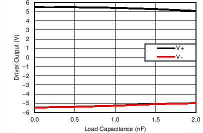 Figure 2. Driver Output vs. Load Capacitance, VCC = 3.3V
VL = 1.8V, RLOAD = 3 kΩ, CH1 = 1 Mbps, CH2 = 32 kbps
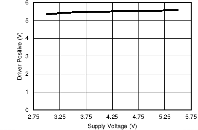 Figure 4. Driver Positive vs. Supply Voltage (Doubler Mode)
1 Mbps, RLOAD = 3 kΩ, CLOAD = 560 pF
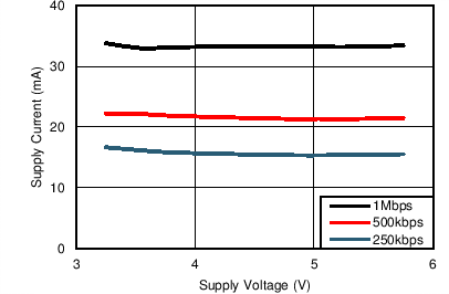 Figure 6. Supply Current vs. Supply Voltage (Doubler Mode)
VL = 1.8 V, RLOAD = 3 kΩ, CLOAD = 1 nF, CH2 = 32 kbps