SCDS225B March 2007 – January 2015 TS3A44159
PRODUCTION DATA.
- 1 Features
- 2 Applications
- 3 Description
- 4 Revision History
- 5 Pin Configuration and Functions
-
6 Specifications
- 6.1 Absolute Maximum Ratings
- 6.2 ESD Ratings
- 6.3 Recommended Operating Conditions
- 6.4 Thermal Information
- 6.5 Electrical Characteristics for 1.8-V Supply
- 6.6 Electrical Characteristics for 2.1-V Supply
- 6.7 Electrical Characteristics for 2.5-V Supply
- 6.8 Electrical Characteristics for 3.3-V Supply
- 6.9 Electrical Characteristics for 4.3-V Supply
- 6.10 Typical Characteristics
- 7 Parameter Measurement Information
- 8 Detailed Description
- 9 Application and Implementation
- 10Power Supply Recommendations
- 11Layout
- 12Device and Documentation Support
- 13Mechanical, Packaging, and Orderable Information
Package Options
Refer to the PDF data sheet for device specific package drawings
Mechanical Data (Package|Pins)
- PW|16
- RGT|16
- RSV|16
Thermal pad, mechanical data (Package|Pins)
Orderable Information
1 Features
- Specified Break-Before-Make Switching
- Low ON-State Resistance (<0.5 Ω)
- Control Inputs Are 1.8-V Logic Compatible
- Low Charge Injection
- Excellent ON-State Resistance Matching
- Low Total Harmonic Distortion (THD)
- 1.65-V to 4.3-V Single-Supply Operation
- Latch-Up Performance Exceeds 100 mA
Per JESD 78, Class II - ESD Performance Tested Per JESD 22
- ±2000-V Human-Body Model
(A114-B, Class II) - ±1000-V Charged-Device Model (C101)
- ±2000-V Human-Body Model
2 Applications
- Cell Phones
- PDAs
- Portable Instrumentation
- Audio and Video Signal Routing
- Low-Voltage Data-Acquisition Systems
- Communication Circuits
- Modems
- Hard Drives
- Computer Peripherals
- Wireless Pins and Peripherals
3 Description
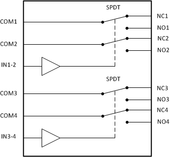
The TS3A44159 is a bidirectional 4-channel single-pole double-throw (SPDT) analog switch with two control inputs, which is designed to operate from 1.65 V to 4.3 V. This device is also known as a 2 channel double-pole double-throw (DPDT) configuration. It offers low ON-state resistance and excellent ON-state resistance matching with the break-before-make feature that prevents signal distortion during the transferring of a signal from one channel to another. The device has an excellent total harmonic distortion (THD) performance and consumes very low power. These features make this device suitable for portable audio applications
Device Information(1)
| PART NUMBER | PACKAGE | BODY SIZE (NOM) |
|---|---|---|
| TS3A44159 | TSSOP (16) | 5.00 mm × 4.40 mm |
| VQFN (16) | 3.00 mm × 3.00 mm | |
| UQFN (16) | 2.60 mm × 1.80 mm |
- For all available packages, see the orderable addendum at the end of the datasheet.
Simplified Schematic
4 Revision History
Changes from B Revision (October 2012) to C Revision
- Added Pin Configuration and Functions section, ESD Ratings table, Feature Description section, Device Functional Modes, Application and Implementation section, Power Supply Recommendations section, Layout section, Device and Documentation Support section, and Mechanical, Packaging, and Orderable Information section Go