SCDS225B March 2007 – January 2015 TS3A44159
PRODUCTION DATA.
- 1 Features
- 2 Applications
- 3 Description
- 4 Revision History
- 5 Pin Configuration and Functions
-
6 Specifications
- 6.1 Absolute Maximum Ratings
- 6.2 ESD Ratings
- 6.3 Recommended Operating Conditions
- 6.4 Thermal Information
- 6.5 Electrical Characteristics for 1.8-V Supply
- 6.6 Electrical Characteristics for 2.1-V Supply
- 6.7 Electrical Characteristics for 2.5-V Supply
- 6.8 Electrical Characteristics for 3.3-V Supply
- 6.9 Electrical Characteristics for 4.3-V Supply
- 6.10 Typical Characteristics
- 7 Parameter Measurement Information
- 8 Detailed Description
- 9 Application and Implementation
- 10Power Supply Recommendations
- 11Layout
- 12Device and Documentation Support
- 13Mechanical, Packaging, and Orderable Information
Package Options
Refer to the PDF data sheet for device specific package drawings
Mechanical Data (Package|Pins)
- PW|16
- RGT|16
- RSV|16
Thermal pad, mechanical data (Package|Pins)
Orderable Information
9 Application and Implementation
NOTE
Information in the following applications sections is not part of the TI component specification, and TI does not warrant its accuracy or completeness. TI’s customers are responsible for determining suitability of components for their purposes. Customers should validate and test their design implementation to confirm system functionality.
9.1 Application Information
The switches are bidirectional, so the NO, NC, and COM pins can be used as either inputs or outputs.
9.2 Typical Application
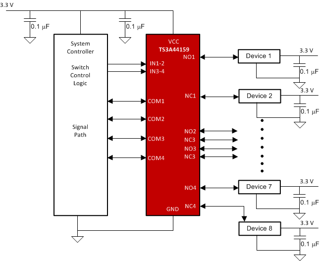 Figure 28. Typical Application Diagram
9.2.1 Design Requirements
Ensure that all of the signals passing through the switch are with in the specified ranges to ensure proper performance.
Table 2. Design Parameters
| DESIGN PARAMETERS | EXAMPLE VALUES | |||
|---|---|---|---|---|
| Analog Voltage | 4.3 V | |||
| Digital Input Voltage | 4.3 V | |||
9.2.2 Detailed Design Procedure
The TS3A44159 can be properly operated without any external components. However, TI recommends to connect unused pins to the ground through a 50-Ω resistor to prevent signal reflections back into the device. TI also recommends that the digital control pins (INX) be pulled up to VCC or down to GND to avoid undesired switch positions that could result from the floating pin.
9.2.3 Application Curve
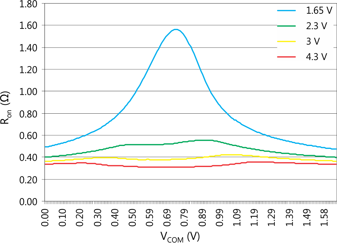 Figure 29. Ron vs VCOM (All Voltages)