SCDS176B SEPTEMBER   2004  – October 2019 TS3L110

PRODUCTION DATA.  

  1. Features
  2. Applications
  3. Description
    1.     Logic Diagram (Positive Logic)
  4. Revision History
  5. Pin Configuration and Functions
    1.     Pin Functions
  6. Specifications
    1. 6.1 Absolute Maximum Ratings
    2. 6.2 ESD Ratings
    3. 6.3 Recommended Operating Conditions
    4. 6.4 Thermal Information
    5. 6.5 Electrical Characteristics
    6. 6.6 Switching Characteristics
    7. 6.7 Dynamic Characteristics
    8. 6.8 Typical Characteristics
  7. Parameter Measurement Information
  8. Detailed Description
    1. 8.1 Overview
    2. 8.2 Functional Block Diagram
    3. 8.3 Feature Description
    4. 8.4 Device Functional Modes
  9. Application and Implementation
    1. 9.1 Application Information
    2. 9.2 Typical Application
      1. 9.2.1 Design Requirements
      2. 9.2.2 Detailed Design Procedure
      3. 9.2.3 Application Curves
  10. 10Power Supply Recommendations
  11. 11Layout
    1. 11.1 Layout Guidelines
    2. 11.2 Layout Example
  12. 12Device and Documentation Support
    1. 12.1 Receiving Notification of Documentation Updates
    2. 12.2 Community Resources
    3. 12.3 Trademarks
    4. 12.4 Electrostatic Discharge Caution
    5. 12.5 Glossary
  13. 13Mechanical, Packaging, and Orderable Information

Package Options

Refer to the PDF data sheet for device specific package drawings

Mechanical Data (Package|Pins)
  • PW|16
  • DBQ|16
  • RGY|16
  • D|16
  • DGV|16
Thermal pad, mechanical data (Package|Pins)
Orderable Information

Typical Characteristics

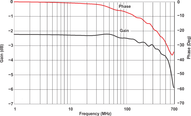
TS3L110 gn_phs_cds176.gif
Phase at 627 MHz, −36 Deg
Gain −3 dB at 627 MHz
Figure 1. Gain and Phase vs Frequency
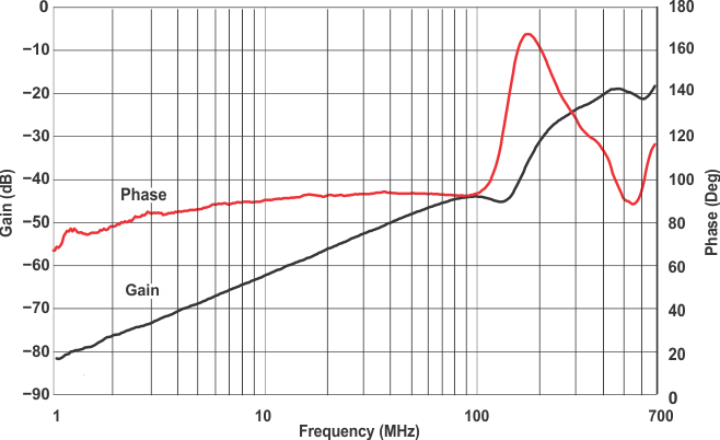
TS3L110 crs_v_fre_cds176.gif
Phase at 250 MHz, 137.92 Deg
Gain −26 dB at 250 MHZ
Figure 3. Crosstalk vs Frequency
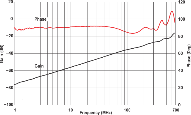
TS3L110 offiso_v_fre_cds176.gif
Phase at 250 MHz, 88.2 Deg
Gain −28.5 dB at 250 MHz
Figure 2. OFF Isolation vs Frequency
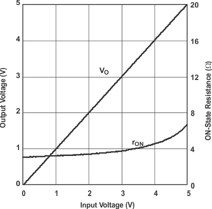
TS3L110 ovol_nvol_cds176.gif
Figure 4. Output Voltage and ON-State Resistance vs Input Voltage