SCDS348C September 2013 – March 2017 TS3USB3031
PRODUCTION DATA.
- 1 Features
- 2 Applications
- 3 Description
- 4 Revision History
- 5 Pin Configuration and Functions
- 6 Specifications
- 7 Parameter Measurement Information
- 8 Detailed Description
- 9 Application and Implementation
- 10Power Supply Recommendations
- 11Layout
- 12Device and Documentation Support
- 13Mechanical, Packaging, and Orderable Information
Package Options
Mechanical Data (Package|Pins)
- RMG|12
Thermal pad, mechanical data (Package|Pins)
Orderable Information
8 Detailed Description
8.1 Overview
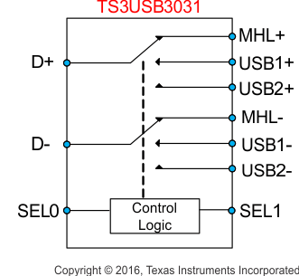
The TS3USB3031 device is a 2-channel, 1:3 multiplexer that includes a high-speed Mobile High-Definition Link (MHL) or Mobility Display Port (MyDP) switch and USB 2.0 High-Speed (480 Mbps) switches in the same package. This device is used in many high-speed differential 1:3 mux applications.
8.3 Feature Description
8.3.1 IOFF Protection
IOFF protection precents current leakage through the device when Vcc = 0 V This allows signals to be present on the D± and USB/MHL± pins before the device is powered up without damaging the device or system.
8.3.2 1.8-V Compatible Logic
The TS3USB3031 device supports 1.8-V logic irrespective to the supply voltage applied to the IC.
8.3.3 Overvoltage Tolerant (OVT)
The D± and USB/MHL± pins of the device can support signals up to 5.5 V without damaging the device. This protects the TS3USB3031 in case the VBUS pin of the USB connector is shorted to the signal path without additional components added.
8.4 Device Functional Modes
Table 1 lists the functional modes of the TS3USB3031.
Table 1. Function Table
| SEL1 | SEL0 | SWITCH STATUS |
|---|---|---|
| Low | Low | D+/D– connected to USB1+/USB1– |
| Low | High | D+/D– connected to USB2+/USB2– |
| High | Low | D+/D– connected to MHL+/MHL– |
| High | High | USB and MHL switches in High-Z |
