SCES707C August 2008 – December 2016 TS5A12301E
PRODUCTION DATA.
- 1 Features
- 2 Applications
- 3 Description
- 4 Revision History
- 5 Pin Configuration and Functions
- 6 Specifications
- 7 Parameter Measurement Information
- 8 Detailed Description
- 9 Application and Implementation
- 10Power Supply Recommendations
- 11Layout
- 12Device and Documentation Support
- 13Mechanical, Packaging, and Orderable Information
Package Options
Mechanical Data (Package|Pins)
- YFP|6
Thermal pad, mechanical data (Package|Pins)
Orderable Information
9 Application and Implementation
NOTE
Information in the following applications sections is not part of the TI component specification, and TI does not warrant its accuracy or completeness. TI’s customers are responsible for determining suitability of components for their purposes. Customers should validate and test their design implementation to confirm system functionality.
9.1 Application Information
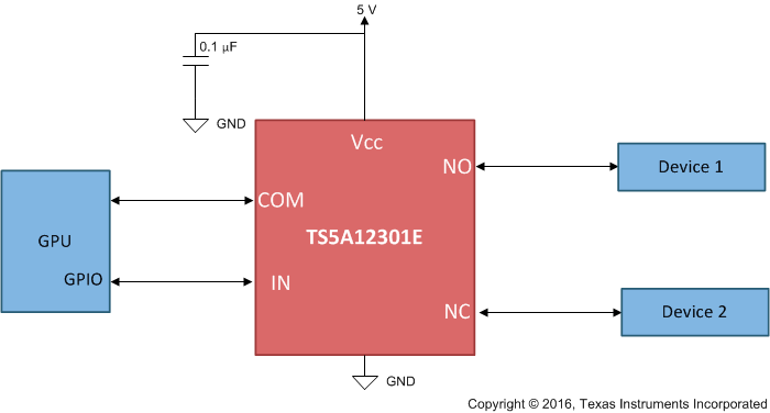
The switch is bidirectional, so the NO, NC, and COM pins may be used as either inputs or outputs.
9.2 Typical Application
 Figure 23. Application Schematic
9.2.1 Design Requirements
This TS5A12301E application may be properly operated without any external components. Unused pins (for example, COM, NC, and NO) may be left floating. Digital control pin (IN) has an integrated 6-MΩ pulldown resistor, so no external component is required to keep the logic pin in a known state.
9.2.2 Detailed Design Procedure
To ensure proper performance, keep all signals passing through the switch within the ranges specified in Recommended Operating Conditions.
9.2.3 Application Curve

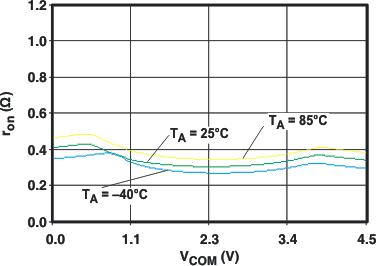
| VCC = 4.5 V |