SCDS336C November 2012 – October 2016 TS5A3159-Q1
PRODUCTION DATA.
- 1 Features
- 2 Applications
- 3 Description
- 4 Revision History
- 5 Pin Configuration and Functions
-
6 Specifications
- 6.1 Absolute Maximum Ratings
- 6.2 ESD Ratings
- 6.3 Recommended Operating Conditions
- 6.4 Thermal Information
- 6.5 Electrical Characteristics for 5-V Supply
- 6.6 Electrical Characteristics for 3.3-V Supply
- 6.7 Electrical Characteristics For 2.5-V Supply
- 6.8 Electrical Characteristics For 1.8-V Supply
- 6.9 Typical Characteristics
- 7 Parameter Measurement Information
- 8 Detailed Description
- 9 Applications and Implementation
- 10Power Supply Recommendations
- 11Layout
- 12Device and Documentation Support
- 13Mechanical, Packaging, and Orderable Information
Package Options
Refer to the PDF data sheet for device specific package drawings
Mechanical Data (Package|Pins)
- DBV|6
Thermal pad, mechanical data (Package|Pins)
Orderable Information
8 Detailed Description
8.1 Overview
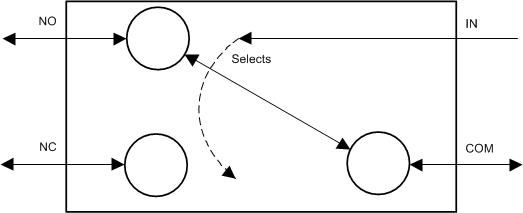
The TS5A3159-Q1 is a single-pole double-throw (SPDT) analog switch designed to operate from 1.65 V to 5.5 V. Either the NO or the NC pin is shorted to the COM pin, depending on the logic level input to the IN pin.
8.2 Functional Block Diagram

8.3 Feature Description
The main feature of this device is the excellent total harmonic distortion performance and low power consumption. Additionally, the NO, NC, and COM pins can be used as either inputs or outputs.
Table 2. Summary Of Characteristics(1)
(1) V+ = 5 V and TA = 25°C
8.4 Device Functional Modes
Table 3 lists the functions for the TS5A3159-Q1 device.
Table 3. Function Table
| IN | NC TO COM, COM TO NC |
NO TO COM, COM TO NO |
|---|---|---|
| L | ON | OFF |
| H | OFF | ON |