SCDS357A July 2014 – December 2014 TS5A3166-Q1
PRODUCTION DATA.
- 1 Features
- 2 Applications
- 3 Description
- 4 Simplified Schematic
- 5 Revision History
- 6 Pin Configuration and Functions
-
7 Specifications
- 7.1 Absolute Maximum Ratings
- 7.2 ESD Ratings
- 7.3 Recommended Operating Conditions
- 7.4 Thermal Information
- 7.5 Electrical Characteristics for 5-V Supply
- 7.6 Electrical Characteristics for 3.3-V Supply
- 7.7 Electrical Characteristics for 2.5-V Supply
- 7.8 Electrical Characteristics for 1.8-V Supply
- 7.9 Typical Characteristics
- 8 Parameter Measurement Information
- 9 Detailed Description
- 10Application and Implementation
- 11Power Supply Recommendations
- 12Layout
- 13Device and Documentation Support
- 14Mechanical, Packaging, and Orderable Information
Package Options
Mechanical Data (Package|Pins)
- DCK|5
Thermal pad, mechanical data (Package|Pins)
Orderable Information
10 Application and Implementation
NOTE
Information in the following applications sections is not part of the TI component specification, and TI does not warrant its accuracy or completeness. TI’s customers are responsible for determining suitability of components for their purposes. Customers should validate and test their design implementation to confirm system functionality.
10.1 Application Information
SPST analog switch is a basic component that could be used in any electrical system design. The following are some basic applications that utilize the TS5A3166, more detailed applications may be found in the Typical Application section.
- Gain-control circuit for amplifier
- Additional details are available in the Typical Application section.
- Improve lock time of a PLL by changing the time constant
- Example Diagram:
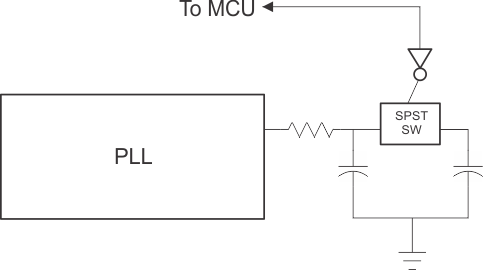 Figure 22. Improved Lock Time Circuit Simplified Block Diagram
- Improve power consumption for PLL
- Example Diagram:
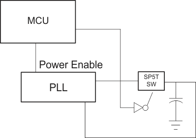 Figure 23. PLL Improved Power Consumption Simplified Block Diagram
10.2 Typical Application
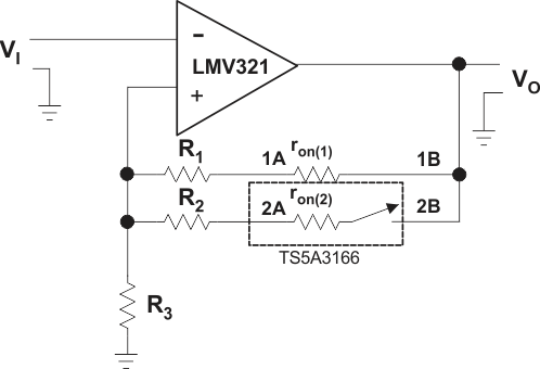 Figure 24. Gain-Control Circuit for OP Amplifier
10.2.1 Design Requirements
Place a switch in series with the input of the op amp. Since the op amp input impedance is very large, a switch on ron(1) is irrelevant.
10.2.2 Detailed Design Procedure
By choosing values of R1 and R2, such that Rx >> ron(x), ron of TS5A3166 can be ignored. The gain of op amp can be calculated as follow:
10.2.3 Application Curves
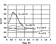 Figure 25. ron vs VCOM
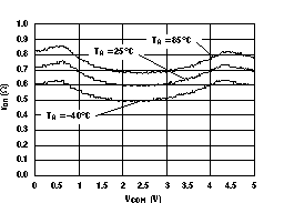 Figure 27. ron vs VCOM (V+ = 5 V)
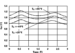 Figure 26. ron vs VCOM (V+ = 3 V)