SCDS357A July 2014 – December 2014 TS5A3166-Q1
PRODUCTION DATA.
- 1 Features
- 2 Applications
- 3 Description
- 4 Simplified Schematic
- 5 Revision History
- 6 Pin Configuration and Functions
-
7 Specifications
- 7.1 Absolute Maximum Ratings
- 7.2 ESD Ratings
- 7.3 Recommended Operating Conditions
- 7.4 Thermal Information
- 7.5 Electrical Characteristics for 5-V Supply
- 7.6 Electrical Characteristics for 3.3-V Supply
- 7.7 Electrical Characteristics for 2.5-V Supply
- 7.8 Electrical Characteristics for 1.8-V Supply
- 7.9 Typical Characteristics
- 8 Parameter Measurement Information
- 9 Detailed Description
- 10Application and Implementation
- 11Power Supply Recommendations
- 12Layout
- 13Device and Documentation Support
- 14Mechanical, Packaging, and Orderable Information
Package Options
Mechanical Data (Package|Pins)
- DCK|5
Thermal pad, mechanical data (Package|Pins)
Orderable Information
7 Specifications
7.1 Absolute Maximum Ratings(1)(2)
over operating free-air temperature range (unless otherwise noted)| MIN | MAX | UNIT | |||
|---|---|---|---|---|---|
| V+ | Supply voltage range(3) | –0.5 | 6.5 | V | |
| VNO
VCOM |
Analog voltage range(3)(4)(5) | –0.5 | V+ + 0.5 | V | |
| IK | Analog port diode current | VNO, VCOM < 0 | –50 | mA | |
| INO
ICOM |
On-state switch current | VNO, VCOM = 0 to V+ | –200 | 200 | mA |
| On-state peak switch current(6) | –400 | 400 | |||
| VI | Digital input voltage range(3)(4) | –0.5 | 6.5 | V | |
| IIK | Digital clamp current | VI < 0 | –50 | mA | |
| I+ | Continuous current through V+ | 100 | mA | ||
| IGND | Continuous current through GND | –100 | mA | ||
| Tstg | Storage temperature range | –65 | 150 | °C | |
(1) Stresses beyond those listed under "absolute maximum ratings" may cause permanent damage to the device. These are stress ratings only, and functional operation of the device at these or any other conditions beyond those indicated under "recommended operating conditions" is not implied. Exposure to absolute-maximum-rated conditions for extended periods may affect device reliability.
(2) The algebraic convention, whereby the most negative value is a minimum and the most positive value is a maximum
(3) All voltages are with respect to ground, unless otherwise specified.
(4) The input and output voltage ratings may be exceeded if the input and output clamp-current ratings are observed.
(5) This value is limited to 5.5 V maximum.
(6) Pulse at 1-ms duration < 10% duty cycle.
7.2 ESD Ratings
| VALUE | UNIT | |||
|---|---|---|---|---|
| V(ESD) | Electrostatic discharge | Human-body model (HBM), per AEC Q100-002(1) | ±2000 | V |
| Charged-device model (CDM), per AEC Q100-011 | ±1000 | |||
(1) AEC Q100-002 indicates that HBM stressing shall be in accordance with the ANSI/ESDA/JEDEC JS-001 specification.
7.3 Recommended Operating Conditions
over operating free-air temperature range (unless otherwise noted)| MIN | MAX | UNIT | ||
|---|---|---|---|---|
| VI/O | Input/output voltage | 0 | 5.5 | V |
| V+ | Supply voltage | 0 | 5.5 | V |
| VI | Control Input Voltage | 0 | 5.5 | V |
| TA | Operating free-air temperature | –40 | 125 | °C |
7.4 Thermal Information
| THERMAL METRIC(1) | TS5A3166-Q1 | UNIT | |
|---|---|---|---|
| DCK | |||
| 5 PINS | |||
| RθJA | Junction-to-ambient thermal resistance | 283.1 | °C/W |
| RθJC(top) | Junction-to-case (top) thermal resistance | 92.2 | |
| RθJB | Junction-to-board thermal resistance | 60.8 | |
| ψJT | Junction-to-top characterization parameter | 1.7 | |
| ψJB | Junction-to-board characterization parameter | 60.0 | |
(1) For more information about traditional and new thermal metrics, see the IC Package Thermal Metrics application report, SPRA953.
7.5 Electrical Characteristics for 5-V Supply(1)
V+ = 4.5 V to 5.5 V, TA = –40°C to 85°C (unless otherwise noted)| PARAMETER | SYMBOL | TEST CONDITIONS | TA | V+ | 85°C | 125°C | UNIT | |||||
|---|---|---|---|---|---|---|---|---|---|---|---|---|
| MIN | TYP | MAX | MIN | TYP | MAX | |||||||
| Analog Switch | ||||||||||||
| Analog signal range | VCOM, VNO |
0 | V+ | 0 | V+ | V | ||||||
| Peak ON resistance | rpeak | 0 ≤ VNO ≤ V+, ICOM = –100 mA, |
Switch ON, See Figure 13 |
25°C | 4.5 V | 0.8 | 1.1 | 0.8 | 1.1 | Ω | ||
| Full | 1.2 | 1.44 | ||||||||||
| ON-state resistance | ron | VNO = 2.5 V, ICOM = –100 mA, |
Switch ON, See Figure 13 |
25°C | 4.5 V | 0.7 | 0.9 | 0.7 | 0.9 | Ω | ||
| Full | 1 | 1.2 | ||||||||||
| ON-state resistance flatness |
ron(flat) | 0 ≤ VNO ≤ V+, ICOM = –100 mA, |
Switch ON, See Figure 13 |
25°C | 4.5 V | 0.15 | 0.15 | Ω | ||||
| VNO = 1 V, 1.5 V, 2.5 V, ICOM = –100 mA, |
25°C | 0.09 | 0.15 | 0.09 | 0.15 | |||||||
| Full | 0.15 | 0.18 | ||||||||||
| NO OFF leakage current |
INO(OFF) | VNO = 1 V, VCOM = 4.5 V, or VNO = 4.5 V, VCOM = 1 V, |
Switch OFF, See Figure 14 |
25°C | 5.5 V | –20 | 4 | 20 | –80 | 4 | 80 | nA |
| Full | –100 | 100 | –400 | 400 | ||||||||
| INO(PWROFF) | VNO = 0 to 5.5 V, VCOM = 5.5 V to 0, |
25°C | 0 V | –5 | 0.4 | 5 | –5 | 0.4 | 5 | μA | ||
| Full | –15 | 15 | –30 | 30 | ||||||||
| COM OFF leakage current |
ICOM(OFF) | VCOM = 1 V, VNO = 4.5 V, or VCOM = 4.5 V, VNO = 1 V, |
Switch OFF, See Figure 14 |
25°C | 5.5 V | –20 | 4 | 20 | –80 | 4 | 80 | nA |
| Full | –100 | 100 | –400 | 400 | ||||||||
| ICOM(PWROFF) | VCOM = 5.5 V to 0, VNO = 0 to 5.5 V, |
25°C | 0 V | –5 | 0.4 | 5 | –5 | 0.4 | 5 | μA | ||
| Full | –15 | 15 | –30 | 30 | ||||||||
| NO ON leakage current |
INO(ON) | VNO = 1 V, VCOM = Open, or VNO = 4.5 V, VCOM = Open, |
Switch ON, See Figure 15 |
25°C | 5.5 V | –2 | 0.3 | 2 | –80 | 0.3 | 80 | nA |
| Full | –20 | 20 | –400 | 400 | ||||||||
| COM ON leakage current |
ICOM(ON) | VCOM = 1 V, VNO = Open, or VCOM = 4.5 V, VNO = Open, |
Switch ON, See Figure 15 |
25°C | 5.5 V | –2 | 0.3 | 2 | –80 | 0.3 | 80 | nA |
| Full | –20 | 20 | –400 | 400 | ||||||||
| Digital Control Inputs (IN) | ||||||||||||
| Input logic high | VIH | Full | 2.4 | 5.5 | 2.4 | 5.5 | V | |||||
| Input logic low | VIL | Full | 0 | 0.8 | 0 | 0.8 | V | |||||
| Input leakage current |
IIH, IIL | VI = 5.5 V or 0 | 25°C | 5.5 V | –2 | 0.3 | 2 | nA | ||||
| Full | –20 | 20 | –400 | 400 | ||||||||
| Dynamic | ||||||||||||
| Turn-on time | tON | VCOM = V+, RL = 50 Ω, |
CL = 35 pF, See Figure 17 |
25°C | 5 V | 2.5 | 4.5 | 7 | 2.5 | 4.5 | 7 | ns |
| Full | 4.5 V to 5.5 V |
1.5 | 7.5 | 1.5 | 7.5 | |||||||
| Turn-off time | tOFF | VCOM = V+, RL = 50 Ω, |
CL = 35 pF, See Figure 17 |
25°C | 5 V | 6 | 9 | 11.5 | 6 | 9 | 11.5 | ns |
| Full | 4.5 V to 5.5 V |
4 | 12.5 | 4 | 12.5 | |||||||
| Charge injection | QC | VGEN = 0, RGEN = 0 , |
CL = 1 nF, See Figure 20 |
25°C | 5 V | 1 | 1 | pC | ||||
| NO OFF capacitance |
CNO(OFF) | VNO = V+ or GND, Switch OFF, |
See Figure 16 | 25°C | 5 V | 19 | 19 | pF | ||||
| COM OFF capacitance |
CCOM(OFF) | VCOM = V+ or GND, Switch OFF, |
See Figure 16 | 25°C | 5 V | 18 | 18 | pF | ||||
| NO ON capacitance |
CNO(ON) | VNO = V+ or GND, Switch ON, |
See Figure 16 | 25°C | 5 V | 35.5 | 35.5 | pF | ||||
| COM ON capacitance |
CCOM(ON) | VCOM = V+ or GND, Switch ON, |
See Figure 16 | 25°C | 5 V | 35.5 | 35.5 | pF | ||||
| Digital input capacitance |
CI | VI = V+ or GND, | See Figure 16 | 25°C | 5 V | 2 | 2 | pF | ||||
| Bandwidth | BW | RL = 50 Ω, Switch ON, |
See Figure 18 | 25°C | 5 V | 200 | 200 | MHz | ||||
| OFF isolation | OISO | RL = 50 Ω, f = 1 MHz, |
Switch OFF, See Figure 19 |
25°C | 5 V | –64 | –64 | dB | ||||
| Total harmonic distortion |
THD | RL = 600 Ω, CL = 50 pF, |
f = 20 Hz to 20 kHz, See Figure 21 |
25°C | 5 V | 0.005 | 0.005 | % | ||||
| Supply | ||||||||||||
| Positive supply current |
I+ | VI = V+ or GND, | Switch ON or OFF | 25°C | 5.5 V | 0.01 | 0.1 | 0.01 | 0.1 | μA | ||
| Full | 0.5 | 0.8 | ||||||||||
(1) The algebraic convention, whereby the most negative value is a minimum and the most positive value is a maximum.
7.6 Electrical Characteristics for 3.3-V Supply(1)
V+ = 3 V to 3.6 V, TA = –40°C to 85°C (unless otherwise noted)| PARAMETER | SYMBOL | TEST CONDITIONS | TA | V+ | 85°C | 125°C | UNIT | |||||
|---|---|---|---|---|---|---|---|---|---|---|---|---|
| MIN | TYP | MAX | MIN | TYP | MAX | |||||||
| Analog Switch | ||||||||||||
| Analog signal range | VCOM, VNO |
0 | V+ | 0 | V+ | V | ||||||
| Peak ON resistance | rpeak | 0 ≤ VNO ≤ V+, ICOM = –100 mA, |
Switch ON, See Figure 13 |
25°C | 3 V | 1.1 | 1.5 | 1.1 | 1.5 | Ω | ||
| Full | 1.7 | 2.07 | ||||||||||
| ON-state resistance | ron | VNO = 2 V, ICOM = –100 mA, |
Switch ON, See Figure 13 |
25°C | 3 V | 1 | 1.4 | 1 | 1.4 | Ω | ||
| Full | 1.5 | 1.8 | ||||||||||
| ON-state resistance flatness |
ron(flat) | 0 ≤ VNO ≤ V+, ICOM = –100 mA, |
Switch ON, See Figure 13 |
25°C | 3 V | 0.3 | 0.3 | Ω | ||||
| VNO = 2 V, 0.8 V, ICOM = –100 mA, |
25°C | 0.09 | 0.15 | 0.09 | 0.15 | |||||||
| Full | 0.15 | 0.18 | ||||||||||
| NO OFF leakage current |
INO(OFF) | VNO = 1 V, VCOM = 3 V, or VNO = 3 V, VCOM = 1 V, |
Switch OFF, See Figure 14 |
25°C | 3.6 V | –2 | 0.5 | 2 | –2 | 0.5 | 2 | nA |
| Full | –20 | 20 | –360 | 360 | ||||||||
| INO(PWROFF) | VNO = 0 to 3.6 V, VCOM = 3.6 V to 0, |
25°C | 0 V | –1 | 0.1 | 1 | –1 | 0.1 | 1 | μA | ||
| Full | –5 | 5 | –27 | 27 | ||||||||
| COM OFF leakage current |
ICOM(OFF) | VCOM = 1 V, VNO = 3 V, or VCOM = 3 V, VNO = 1 V, |
Switch OFF, See Figure 14 |
25°C | 3.6 V | –2 | 0.5 | 2 | –72 | 0.5 | 72 | nA |
| Full | –20 | 20 | –360 | 360 | ||||||||
| ICOM(PWROFF) | VCOM = 3.6 V to 0, VNO = 0 to 3.6 V, |
25°C | 0 V | –1 | 0.1 | 1 | –2 | 0.1 | 2 | μA | ||
| Full | –5 | 5 | –27 | 27 | ||||||||
| NO ON leakage current |
INO(ON) | VNO = 1 V, VCOM = Open, or VNO = 3 V, VCOM = Open, |
Switch ON, See Figure 15 |
25°C | 3.6 V | –2 | 0.2 | 2 | –72 | 72 | nA | |
| Full | –20 | 20 | –360 | 360 | ||||||||
| COM ON leakage current |
ICOM(ON) | VCOM = 1 V, VNO = Open, or VCOM = 3 V, VNO = Open, |
Switch ON, See Figure 15 |
25°C | 3.6 V | –2 | 0.2 | 2 | –72 | 72 | nA | |
| Full | –20 | 20 | –360 | 360 | ||||||||
| Digital Control Inputs (IN) | ||||||||||||
| Input logic high | VIH | Full | 2 | 5.5 | 2 | 5.5 | V | |||||
| Input logic low | VIL | Full | 0 | 0.8 | 0 | 0.8 | V | |||||
| Input leakage current | IIH, IIL | VI = 5.5 V or 0 | 25°C | 3.6 V | –2 | 0.3 | 2 | nA | ||||
| Full | –20 | 20 | –360 | 360 | ||||||||
| Dynamic | ||||||||||||
| Turn-on time | tON | VCOM = V+, RL = 50 Ω, |
CL = 35 pF, See Figure 17 |
25°C | 3.3 V | 2 | 5 | 10 | 2 | 5 | 10 | ns |
| Full | 3 V to 3.6 V |
1.5 | 11 | 1.5 | 11 | |||||||
| Turn-off time | tOFF | VCOM = V+, RL = 50 Ω, |
CL = 35 pF, See Figure 17 |
25°C | 3.3 V | 6.5 | 9 | 12 | 6.5 | 9 | 12 | ns |
| Full | 3 V to 3.6 V |
4 | 13 | 4 | 13 | |||||||
| Charge injection | QC | VGEN = 0, RGEN = 0, |
CL = 1 nF, See Figure 21 |
25°C | 3.3 V | 1 | 1 | pC | ||||
| NO OFF capacitance |
CNO(OFF) | VNO = V+ or GND, Switch OFF, |
See Figure 16 | 25°C | 3.3 V | 19 | 19 | pF | ||||
| COM OFF capacitance |
CCOM(OFF) | VCOM = V+ or GND, Switch OFF, |
See Figure 16 | 25°C | 3.3 V | 18 | 18 | pF | ||||
| NO ON capacitance |
CNO(ON) | VNO = V+ or GND, Switch ON, |
See Figure 16 | 25°C | 3.3 V | 36 | 36 | pF | ||||
| COM ON capacitance |
CCOM(ON) | VCOM = V+ or GND, Switch ON, |
See Figure 16 | 25°C | 3.3 V | 36 | 36 | pF | ||||
| Digital input capacitance |
CI | VI = V+ or GND, | See Figure 16 | 25°C | 3.3 V | 2 | 2 | pF | ||||
| Bandwidth | BW | RL = 50 Ω, Switch ON, |
See Figure 18 | 25°C | 3.3 V | 200 | 200 | MHz | ||||
| OFF isolation | OISO | RL = 50 Ω, f = 1 MHz, |
Switch OFF, See Figure 19 |
25°C | 3.3 V | –64 | –64 | dB | ||||
| Total harmonic distortion |
THD | RL = 600 Ω, CL = 50 pF, |
f = 20 Hz to 20 kHz, See Figure 21 |
25°C | 3.3 V | 0.01 | 0.01 | % | ||||
| Supply | ||||||||||||
| Positive supply current |
I+ | VI = V+ or GND, | Switch ON or OFF | 25°C | 3.6 V | 0.01 | 0.1 | 0.01 | 0.1 | μA | ||
| Full | 0.25 | 0.7 | ||||||||||
(1) The algebraic convention, whereby the most negative value is a minimum and the most positive value is a maximum
7.7 Electrical Characteristics for 2.5-V Supply(1)
V+ = 2.3 V to 2.7 V, TA = –40°C to 85°C (unless otherwise noted)| PARAMETER | SYMBOL | TEST CONDITIONS | TA | V+ | 85°C | 125°C | UNIT | |||||
|---|---|---|---|---|---|---|---|---|---|---|---|---|
| MIN | TYP | MAX | MIN | TYP | MAX | |||||||
| Analog Switch | ||||||||||||
| Analog signal range | VCOM, VNO |
2.3 V | 0 | V+ | 0 | V+ | V | |||||
| Peak ON resistance | rpeak | 0 ≤ VNO ≤ V+, ICOM = –100 mA, |
Switch ON, See Figure 13 |
25°C | 2.3 V | 1.8 | 2.4 | 1.8 | 2.4 | Ω | ||
| Full | 2.6 | 3.1 | ||||||||||
| ON-state resistance | ron | VNO = 2 V, ICOM = –100 mA, |
Switch ON, See Figure 13 |
25°C | 2.3 V | 1.2 | 2.1 | 1.2 | 2.1 | Ω | ||
| Full | 2.4 | 2.88 | ||||||||||
| ON-state resistance flatness |
ron(flat) | 0 ≤ VNO ≤ V+, ICOM = –100 mA, |
Switch ON, See Figure 13 |
25°C | 2.3 V | 0.7 | 0.7 | Ω | ||||
| VNO = 2 V, 0.8 V, ICOM = –100 mA, |
25°C | 0.4 | 0.6 | 0.4 | 0.6 | |||||||
| Full | 0.6 | 0.72 | ||||||||||
| NO OFF leakage current |
INO(OFF) | VNO = 1 V, VCOM = 3 V, or VNO = 3 V, VCOM = 1 V, |
Switch OFF, See Figure 14 |
25°C | 2.7 V | –5 | 0.3 | 5 | –64 | 0.3 | 64 | nA |
| Full | –50 | 50 | –320 | 320 | ||||||||
| INO(PWROFF) | VNO = 0 to 3.6 V, VCOM = 3.6 V to 0, |
25°C | 0 V | –2 | 0.05 | 2 | –2 | 0.05 | 2 | μA | ||
| Full | –15 | 15 | –24 | 24 | ||||||||
| COM OFF leakage current |
ICOM(OFF) | VCOM = 1 V, VNO = 3 V, or VCOM = 3 V, VNO = 1 V, |
Switch OFF, See Figure 14 |
25°C | 2.7 V | –5 | 0.3 | 5 | –64 | 0.3 | 64 | nA |
| Full | –50 | 50 | –320 | 320 | ||||||||
| ICOM(PWROFF) | VCOM = 3.6 V to 0, VNO = 0 to 3.6 V, |
25°C | 0 V | –2 | 0.05 | 2 | –2 | 0.05 | 2 | μA | ||
| Full | –15 | 15 | –24 | 24 | ||||||||
| NO ON leakage current |
INO(ON) | VNO = 1 V, VCOM = Open, or VNO = 3 V, VCOM = Open, |
Switch ON, See Figure 15 |
25°C | 2.7 V | –2 | 0.3 | 2 | –64 | 64 | nA | |
| Full | –20 | 20 | –320 | 320 | ||||||||
| COM ON leakage current |
ICOM(ON) | VCOM = 1 V, VNO = Open, or VCOM = 3 V, VNO = Open, |
Switch ON, See Figure 15 |
25°C | 2.7 V | –2 | 0.3 | 2 | –64 | 0.3 | 64 | nA |
| Full | –20 | 20 | –320 | 320 | ||||||||
| Digital Control Inputs (IN1, IN2) | ||||||||||||
| Input logic high | VIH | Full | 1.8 | 5.5 | 1.8 | 5.5 | V | |||||
| Input logic low | VIL | Full | 0 | 0.6 | 0 | 0.6 | V | |||||
| Input leakage current | IIH, IIL | VI = 5.5 V or 0 | 25°C | 2.7 V | –2 | 0.3 | 2 | nA | ||||
| Full | –20 | 20 | –320 | 320 | ||||||||
| Dynamic | ||||||||||||
| Turn-on time | tON | VCOM = V+, RL = 50 Ω, |
CL = 35 pF, See Figure 17 |
25°C | 2.5 V | 2 | 6 | 10 | 2 | 6 | 10 | ns |
| Full | 2.3 V to 2.7 V | 1 | 12 | 1 | 12 | |||||||
| Turn-off time | tOFF | VCOM = V+, RL = 50 Ω, |
CL = 35 pF, See Figure 17 |
25°C | 2.5 V | 4.5 | 8 | 10.5 | 4.5 | 8 | 10.5 | ns |
| Full | 2.3 V to 2.7 V | 3 | 15 | 3 | 15 | |||||||
| Charge injection | QC | VGEN = 0, RGEN = 0, |
CL = 1 nF, See Figure 21 |
25°C | 2.5 V | 4 | 4 | pC | ||||
| NO OFF capacitance |
CNO(OFF) | VNO = V+ or GND, Switch OFF, |
See Figure 16 | 25°C | 2.5 V | 19.5 | 19.5 | pF | ||||
| COM OFF capacitance |
CCOM(OFF) | VCOM = V+ or GND, Switch OFF, |
See Figure 16 | 25°C | 2.5 V | 18.5 | 18.5 | pF | ||||
| NO ON capacitance |
CNO(ON) | VNO = V+ or GND, Switch ON, |
See Figure 16 | 25°C | 2.5 V | 36.5 | 36.5 | pF | ||||
| COM ON capacitance |
CCOM(ON) | VCOM = V+ or GND, Switch ON, |
See Figure 16 | 25°C | 2.5 V | 36.5 | 36.5 | pF | ||||
| Digital input capacitance |
CI | VI = V+ or GND, | See Figure 16 | 25°C | 2.5 V | 2 | 2 | pF | ||||
| Bandwidth | BW | RL = 50 Ω, Switch ON, |
See Figure 18 | 25°C | 2.5 V | 150 | 150 | MHz | ||||
| OFF isolation | OISO | RL = 50 Ω, f = 1 MHz, |
Switch OFF, See Figure 19 |
25°C | 2.5 V | –62 | –62 | dB | ||||
| Total harmonic distortion |
THD | RL = 600 Ω, CL = 50 pF, |
f = 20 Hz to 20 kHz, See Figure 21 |
25°C | 2.5 V | 0.02 | 0.02 | % | ||||
| Supply | ||||||||||||
| Positive supply current |
I+ | VI = V+ or GND, | Switch ON or OFF | 25°C | 2.7 V | 0.001 | 0.02 | 0.001 | 0.02 | μA | ||
| Full | 0.25 | 0.6 | ||||||||||
(1) The algebraic convention, whereby the most negative value is a minimum and the most positive value is a maximum
7.8 Electrical Characteristics for 1.8-V Supply(1)
V+ = 1.65 V to 1.95 V, TA = –40°C to 85°C (unless otherwise noted))| PARAMETER | SYMBOL | TEST CONDITIONS | TA | V+ | 85°C | 125°C | UNIT | |||||
|---|---|---|---|---|---|---|---|---|---|---|---|---|
| MIN | TYP | MAX | MIN | TYP | MAX | |||||||
| Analog Switch | ||||||||||||
| Analog signal range | VCOM, VNO |
0 | V+ | 0 | V+ | V | ||||||
| Peak ON resistance | rpeak | 0 ≤ VNO ≤ V+, ICOM = –100 mA, |
Switch ON, See Figure 13 |
25°C | 1.65 V | 4.2 | 25 | 4.2 | 25 | Ω | ||
| Full | 30 | 36 | ||||||||||
| ON-state resistance | ron | VNO = 2 V, ICOM = –100 mA, |
Switch ON, See Figure 13 |
25°C | 1.65 V | 1.6 | 3.9 | 1.6 | 3.9 | Ω | ||
| Full | 4.0 | 4.8 | ||||||||||
| ON-state resistance flatness |
ron(flat) | 0 ≤ VNO ≤ V+, ICOM = –100 mA, |
Switch ON, See Figure 13 |
25°C | 1.65 V | 2.8 | 2.8 | Ω | ||||
| VNO = 2 V, 0.8 V, ICOM = –100 mA, |
25°C | 4.1 | 22 | 4.1 | 22 | |||||||
| Full | 27 | 32.4 | ||||||||||
| NO OFF leakage current |
INO(OFF) | VNO = 1 V, VCOM = 3 V, or VNO = 3 V, VCOM = 1 V, |
Switch OFF, See Figure 14 |
25°C | 1.95 V | –5 | 5 | –58 | 58 | nA | ||
| Full | –50 | 50 | –320 | 320 | ||||||||
| INO(PWROFF) | VNO = 0 to 3.6 V, VCOM = 3.6 V to 0, |
25°C | 0 V | –2 | 2 | –2 | 2 | μA | ||||
| Full | –10 | 10 | –22 | 22 | ||||||||
| COM OFF leakage current |
ICOM(OFF) | VCOM = 1 V, VNO = 3 V, or VCOM = 3 V, VNO = 1 V, |
Switch OFF, See Figure 14 |
25°C | 1.95 V | –5 | 5 | –58 | 58 | nA | ||
| Full | –50 | 50 | –320 | 320 | ||||||||
| ICOM(PWROFF) | VCOM = 0 to 3.6 V, VNO = 3.6 V to 0, |
25°C | 0 V | –2 | 2 | –2 | 2 | μA | ||||
| Full | –10 | 10 | –22 | 22 | ||||||||
| NO ON leakage current |
INO(ON) | VNO = 1 V, VCOM = Open, or VNO = 3 V, VCOM = Open, |
Switch ON, See Figure 15 |
25°C | 1.95 V | –2 | 2 | –58 | 58 | nA | ||
| Full | –20 | 20 | –320 | 320 | ||||||||
| COM ON leakage current |
ICOM(ON) | VCOM = 1 V, VNO = Open, or VCOM = 3 V, VNO = Open, |
Switch ON, See Figure 15 |
25°C | 1.95 V | –2 | 2 | –58 | 58 | nA | ||
| Full | –20 | 20 | –320 | 320 | ||||||||
| Digital Control Inputs (IN1, IN2) | ||||||||||||
| Input logic high | VIH | Full | 1.5 | 5.5 | 1.5 | 5.5 | V | |||||
| Input logic low | VIL | Full | 0 | 0.6 | 0 | 0.6 | V | |||||
| Input leakage current | IIH, IIL | VI = 5.5 V or 0 | 25°C | 1.95 V | –2 | 0.3 | 2 | nA | ||||
| Full | –20 | 20 | –320 | 320 | ||||||||
| Dynamic | ||||||||||||
| Turn-on time | tON | VCOM = V+, RL = 50 Ω, |
CL = 35 pF, See Figure 17 |
25°C | 1.8 V | 3 | 9 | 18 | 3 | 9 | 18 | ns |
| Full | 1.65 V to 1.95 V |
1 | 20 | 1 | 20 | |||||||
| Turn-off time | tOFF | VCOM = V+, RL = 50 Ω, |
CL = 35 pF, See Figure 17 |
25°C | 1.8 V | 5 | 10 | 15.5 | 5 | 10 | 15.5 | ns |
| Full | 1.65 V to 1.95 V |
4 | 18.5 | 4 | 18.5 | |||||||
| Charge injection | QC | VGEN = 0, RGEN = 0, |
CL = 1 nF, See Figure 21 |
25°C | 1.8 V | 2 | 2 | pC | ||||
| NO OFF capacitance |
CNO(OFF) | VNO = V+ or GND, Switch OFF, |
See Figure 16 | 25°C | 1.8 V | 19.5 | 19.5 | pF | ||||
| COM OFF capacitance |
CCOM(OFF) | VCOM = V+ or GND, Switch OFF, |
See Figure 16 | 25°C | 1.8 V | 18.5 | 18.5 | pF | ||||
| NO ON capacitance |
CNO(ON) | VNO = V+ or GND, Switch ON, |
See Figure 16 | 25°C | 1.8 V | 36.5 | 36.5 | pF | ||||
| COM ON capacitance |
CCOM(ON) | VCOM = V+ or GND, Switch ON, |
See Figure 16 | 25°C | 1.8 V | 36.5 | 36.5 | pF | ||||
| Digital input capacitance |
CI | VI = V+ or GND, | See Figure 16 | 25°C | 1.8 V | 2 | 2 | pF | ||||
| Bandwidth | BW | RL = 50 Ω, Switch ON, |
See Figure 18 | 25°C | 1.8 V | 150 | 150 | MHz | ||||
| OFF isolation | OISO | RL = 50 Ω, f = 1 MHz, |
Switch OFF, See Figure 19 |
25°C | 1.8 V | –62 | –62 | dB | ||||
| Total harmonic distortion |
THD | RL = 600 Ω, CL = 50 pF, |
f = 20 Hz to 20 kHz See Figure 21 |
25°C | 1.8 V | 0.055 | 0.055 | % | ||||
| Supply | ||||||||||||
| Positive supply current |
I+ | VI = V+ or GND, | Switch ON or OFF | 25°C | 1.95 V | 0.001 | 0.01 | 0.001 | 0.01 | μA | ||
| Full | 0.15 | 0.6 | ||||||||||
(1) The algebraic convention, whereby the most negative value is a minimum and the most positive value is a maximum
7.9 Typical Characteristics
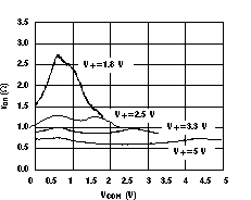 Figure 1. ron vs VCOM
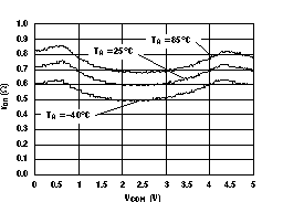 Figure 3. ron vs VCOM (V+ = 5 V)
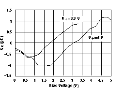 Figure 5. Charge Injection (QC) vs VCOM
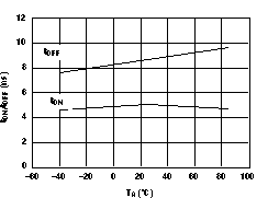 Figure 7. tON and tOFF vs Temperature (V+ = 5 V)
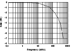 Figure 9. Gain vs Frequency (V+ = 5 V)
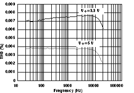 Figure 11. Total Harmonic Distortion vs Frequency
(V+ = 5 V)
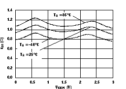 Figure 2. ron vs VCOM (V+ = 3 V)
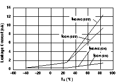 Figure 4. Leakage Current vs Temperature (V+ = 5.5 V)
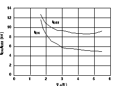 Figure 6. tON and tOFF vs Supply Voltage
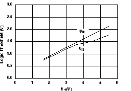 Figure 8. Logic Threshold vs V+
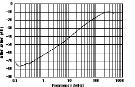 Figure 10. OFF Isolation vs Frequency (V+ = 5 V)
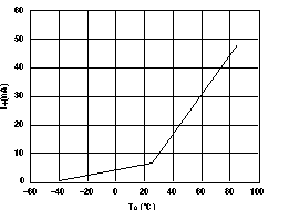 Figure 12. Power-Supply Current vs Temperature
(V+ = 5 V)