SLLSF07 September   2017 TUSB215-Q1

PRODUCTION DATA.  

  1. Features
  2. Applications
  3. Description
  4. Revision History
  5. Pin Configuration and Functions
  6. Specifications
    1. 6.1 Absolute Maximum Ratings
    2. 6.2 ESD Ratings
    3. 6.3 Recommended Operating Conditions
    4. 6.4 Thermal Information
    5. 6.5 Electrical Characteristics
    6. 6.6 Switching Characteristics
    7. 6.7 Typical Characteristics
  7. Detailed Description
    1. 7.1 Overview
    2. 7.2 Functional Block Diagram
    3. 7.3 Feature Description
      1. 7.3.1 EQ
      2. 7.3.2 DC BOOST
      3. 7.3.3 BC1.2 CDP Support
    4. 7.4 Device Functional Modes
      1. 7.4.1 Low Speed (LS) Mode
      2. 7.4.2 Full Speed (FS) Mode
      3. 7.4.3 High Speed (HS) Mode
      4. 7.4.4 Shutdown Mode
      5. 7.4.5 I2C Mode
  8. Application and Implementation
    1. 8.1 Application Information
    2. 8.2 Typical Application
      1. 8.2.1 Design Requirements
      2. 8.2.2 Detailed Design Procedure
        1. 8.2.2.1 Test Procedure to Construct USB High Speed Eye Diagram
          1. 8.2.2.1.1 For a Host Side Application
          2. 8.2.2.1.2 For a Device Side Application
      3. 8.2.3 Application Curves
  9. Power Supply Recommendations
  10. 10Layout
    1. 10.1 Layout Guidelines
    2. 10.2 Layout Example
  11. 11Device and Documentation Support
    1. 11.1 Receiving Notification of Documentation Updates
    2. 11.2 Community Resources
    3. 11.3 Trademarks
    4. 11.4 Electrostatic Discharge Caution
    5. 11.5 Glossary
  12. 12Mechanical, Packaging, and Orderable Information

Package Options

Refer to the PDF data sheet for device specific package drawings

Mechanical Data (Package|Pins)
  • RGY|14
Thermal pad, mechanical data (Package|Pins)
Orderable Information

Layout

Layout Guidelines

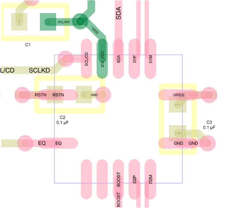
To avoid the need for signal vias, it is highly recommend to route the High Speed traces on the same surface layer than the TUSB215-Q1 is placed. shows an example how one could layout the PCB for TUSB215-Q1.

The layout should use impedance controlled traces to maintain 90 Ω differential impedance for the whole signal path as required per USB 2.0 specification. General guidelines for highspeed signal routing apply.

Layout Example

TUSB215-Q1 layoutsnippet.gif Figure 22. Layout Example