SLVSEG2B September 2018 – September 2022 TVS3301
PRODUCTION DATA
- 1 Features
- 2 Applications
- 3 Description
- 4 Revision History
- 5 Description (continued)
- 6 Device Comparison Table
- 7 Pin Configuration and Functions
- 8 Specifications
- 9 Detailed Description
- 10Application and Implementation
- 11Power Supply Recommendations
- 12Layout
- 13Device and Documentation Support
- 14Mechanical, Packaging, and Orderable Information
Package Options
Mechanical Data (Package|Pins)
- DRB|8
Thermal pad, mechanical data (Package|Pins)
- DRB|8
Orderable Information
3 Description
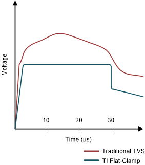
The TVS3301 device shunts up to 27 A of IEC 61000-4-5 fault current to protect systems from high-power transients or lightning strikes. The device survives the common industrial signal line EMC requirement of 1-kV IEC 61000-4-5 open circuit voltage coupled through a 42-Ω impedance. The TVS3301 uses a feedback mechanism to ensure precise flat clamping during a fault, keeping system exposure lower than traditional TVS diodes. The tight voltage regulation allows designers to confidently select system components with a lower voltage tolerance, lowering system costs and complexity without sacrificing robustness. The TVS3301 has a ±33-V operating range to enable operation in systems that require protection against reverse wiring conditions.
In addition, the TVS3301 is available in a small SON footprint designed for space constrained applications, offering a significant size reduction compared to standard SMA and SMB packages. Low device leakage and capacitance ensure a minimal effect on the protected line. To ensure robust protection over the lifetime of the product, TI tests the TVS3301 against 5000 repetitive surge strikes at 125°C with no shift in device performance.
| PART NUMBER | PACKAGE | BODY SIZE (NOM) |
|---|---|---|
| TVS3301 | SON (DRB, 8) | 3.00 mm × 3.00 mm |
 Voltage Clamp Response to
8/20-µs Surge Event
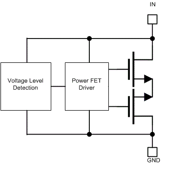
 Functional Block
Diagram