SCES831G September 2011 – May 2019 TXB0304
PRODUCTION DATA.
- 1 Features
- 2 Applications
- 3 Description
- 4 Revision History
- 5 Pin Configuration and Functions
- 6 Specifications
- 7 Parameter Measurement Information
- 8 Detailed Description
- 9 Application and Implementation
- 10Power Supply Recommendations
- 11Layout
- 12Device and Documentation Support
- 13Mechanical, Packaging, and Orderable Information
Package Options
Mechanical Data (Package|Pins)
Thermal pad, mechanical data (Package|Pins)
Orderable Information
5 Pin Configuration and Functions
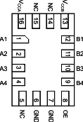
RSV Package
16-Pin UQFN
TXB0304 Top View

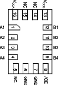
RSV Package
16-Pin UQFN
TXBN0304 Top View

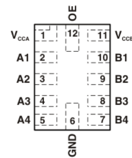
RUT Package
12-Pin UQFN
TXB0304 Top View

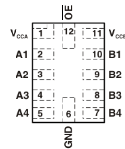
RUT Package
12-Pin UQFN
TXBN0304 Top View

Pin Functions
| PIN | TYPE | DESCRIPTION | ||||||
|---|---|---|---|---|---|---|---|---|
| NAME | TXB0304 | TXBN0304 | ||||||
| RSV | RUT | RSV | RUT | |||||
| A1 | 1 | 2 | 1 | 2 | I/O | Input/output 1 | Referenced to VCCA | |
| A2 | 2 | 3 | 2 | 3 | I/O | Input/output 2 | ||
| A3 | 3 | 4 | 3 | 4 | I/O | Input/output 3 | ||
| A4 | 4 | 5 | 4 | 5 | I/O | Input/output 4 | ||
| B1 | 12 | 10 | 12 | 10 | I/O | Input/output 4 | Referenced to VCCB | |
| B2 | 11 | 9 | 11 | 9 | I/O | Input/output 3 | ||
| B3 | 10 | 8 | 10 | 8 | I/O | Input/output 2 | ||
| B4 | 9 | 7 | 9 | 7 | I/O | Input/output 1 | ||
| GND | 6, 7 | 6 | 6,7 | 6 | GND | Ground | ||
| NC | 5, 14, 15 | — | 5, 14, 15 | — | — | No connection; not internally connected | ||
| OE | 8 | 12 | — | — | I | 3-state output-mode enable. Pull OE (TXB0304) low to place all outputs in 3-state mode. Referenced to VCCA.
|
||
| OE | — | — | 8 | 12 | I | 3-state output-mode enable. Pull OE (TXBN0304) high to place all outputs in 3-state mode.
Referenced to VCCA. |
||
| VCCA | 16 | 1 | 16 | 1 | — | A-port supply voltage 0.9 V ≤ VCCA ≤ 3.6 V | ||
| VCCB | 13 | 11 | 13 | 11 | — | B-port supply voltage 0.9 V ≤ VCCB ≤ 3.6 V | ||