SLUSDD5A April   2019  – December 2020 UC1825B-SP

PRODUCTION DATA  

  1. Features
  2. Applications
  3. Description
  4. Revision History
  5. Pin Configuration and Functions
  6. Specifications
    1. 6.1 Absolute Maximum Ratings
    2. 6.2 ESD Ratings
    3. 6.3 Recommended Operating Conditions
    4. 6.4 Thermal Information
    5. 6.5 Electrical Characteristics
    6. 6.6 Typical Characteristics
  7. Detailed Description
    1. 7.1 Overview
    2. 7.2 Functional Block Diagram
    3. 7.3 Feature Description
      1. 7.3.1 Control Methods
      2. 7.3.2 Synchronization
      3. 7.3.3 High Current Outputs
      4. 7.3.4 Open Loop Test Circuit
    4. 7.4 Device Functional Modes
  8. Application and Implementation
    1. 8.1 Application Information
    2. 8.2 Typical Application
      1. 8.2.1 System Design Theory
        1. 8.2.1.1 Switching Frequency
        2. 8.2.1.2 Transformer
        3. 8.2.1.3 RCD and Diode Clamp
        4. 8.2.1.4 Output Diode
        5. 8.2.1.5 Main Switching MOSFETs
        6. 8.2.1.6 Output Filter and Capacitance
        7. 8.2.1.7 Compensation
        8. 8.2.1.8 Sense Resistor
    3. 8.3 Application Curves
  9. Power Supply Recommendations
  10. 10Layout
    1. 10.1 Layout Guidelines
      1. 10.1.1 Feedback Traces
      2. 10.1.2 Input/Output Capacitors
      3. 10.1.3 Compensation Components
      4. 10.1.4 Traces and Ground Planes
      5. 10.1.5 Ground Planes
    2. 10.2 Layout Example
  11. 11Device and Documentation Support
    1. 11.1 Documentation Support
      1. 11.1.1 Related Documentation
    2. 11.2 Receiving Notification of Documentation Updates
    3. 11.3 Support Resources
    4. 11.4 Trademarks
    5. 11.5 Electrostatic Discharge Caution
    6. 11.6 Glossary
  12. 12Mechanical, Packaging, and Orderable Information

Package Options

Mechanical Data (Package|Pins)
Thermal pad, mechanical data (Package|Pins)
Orderable Information

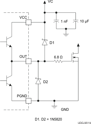
High Current Outputs

Each totem pole output of the UC1825B-SP can deliver a 2-A peak current into a capacitive load. The output can slew a 1000-pF capacitor by 15 V in approximately 20 ns. Separate collector supply (VC) and power ground (PGND) pins help decouple the analog circuitry of the device from the high-power gate drive noise. The use of
3-A Schottky diodes (1N5120, USD245, or equivalent) as shown in the Figure 10-1 from each output to both VC and PGND are recommended. The diodes clamp the output swing to the supply rails, necessary with any type of inductive or capacitive load, typical of a MOSFET gate, as shown in Figure 7-5. Schottky diodes must be used because a low forward voltage drop is required.

Note:

Do not use standard silicon diodes.

GUID-589B3908-08A2-42CE-A6E3-309DCDB2A184-low.gifFigure 7-5 Power MOSFET Drive Circuit