SLUSDD5A April 2019 – December 2020 UC1825B-SP
PRODUCTION DATA
- 1 Features
- 2 Applications
- 3 Description
- 4 Revision History
- 5 Pin Configuration and Functions
- 6 Specifications
- 7 Detailed Description
- 8 Application and Implementation
- 9 Power Supply Recommendations
- 10Layout
- 11Device and Documentation Support
- 12Mechanical, Packaging, and Orderable Information
Package Options
Mechanical Data (Package|Pins)
- HKT|16
- KGD|0
Thermal pad, mechanical data (Package|Pins)
Orderable Information
5 Pin Configuration and Functions
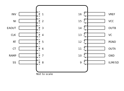
 Figure 5-1 HKT Package
16-Pin CFP
Top View
Table 5-1 Pin Functions
| NAME | NO. | I/O | DESCRIPTION | |
|---|---|---|---|---|
| CLK | 4 | O | Output of the internal oscillator. | |
| CT | 6 | I | Timing capacitor connection pin for oscillator frequency programming. The timing capacitor should be connected to the device ground using minimal trace length. | |
| EAOUT | 3 | O | Output of the error amplifier for compensation. | |
| GND | 10 | — | Analog ground return pin. | |
| ILIM/SD | 9 | I | Input to the current limit comparator and the shutdown comparator. | |
| INV | 1 | I | Inverting input to the error amplifier. | |
| NI | 2 | I | Non-inverting input to the error amplifier. | |
| OUTA | 11 | O | High-current totem pole output A of the on-chip drive stage. | |
| OUTB | 14 | O | High-current totem pole output B of the on-chip drive stage. | |
| PGND | 12 | — | Ground return pin for the output driver stage. | |
| RAMP | 7 | I | Non-inverting input to the PWM comparator with 1.25-V internal input offset. In voltage mode operation this serves as the input voltage feed-forward function by using the CT ramp. In peak current mode operation, this serves as the slope compensation input. | |
| RT | 5 | I | Timing resistor connection pin for oscillator frequency programming. | |
| SS | 8 | I | Soft-start input pin which also doubles as the maximum duty cycle clamp. | |
| VC | 13 | — | Power supply pin for the output stage. This pin should be bypassed with a 0.1-μF monolithic ceramic low ESL capacitor with minimal trace lengths. | |
| VCC | 15 | — | Power supply pin for the device. This pin should be bypassed with a 0.1-μF monolithic ceramic low ESL capacitor with minimal trace lengths. | |
| VREF | 16 | O | 5.1-V reference. For stability, the reference should be bypassed with a 0.1-μF monolithic ceramic low ESL capacitor and minimal trace length to the ground plane. | |
Table 5-2 Bare Die Information
| DIE THICKNESS | BACKSIDE FINISH | BACKSIDE POTENTIAL | BOND PAD METALLIZATION COMPOSITION | BOND PAD THICKNESS |
|---|---|---|---|---|
| 15 mils | Backgrind Si - Finish | GND | AlCu | 2000 nm |
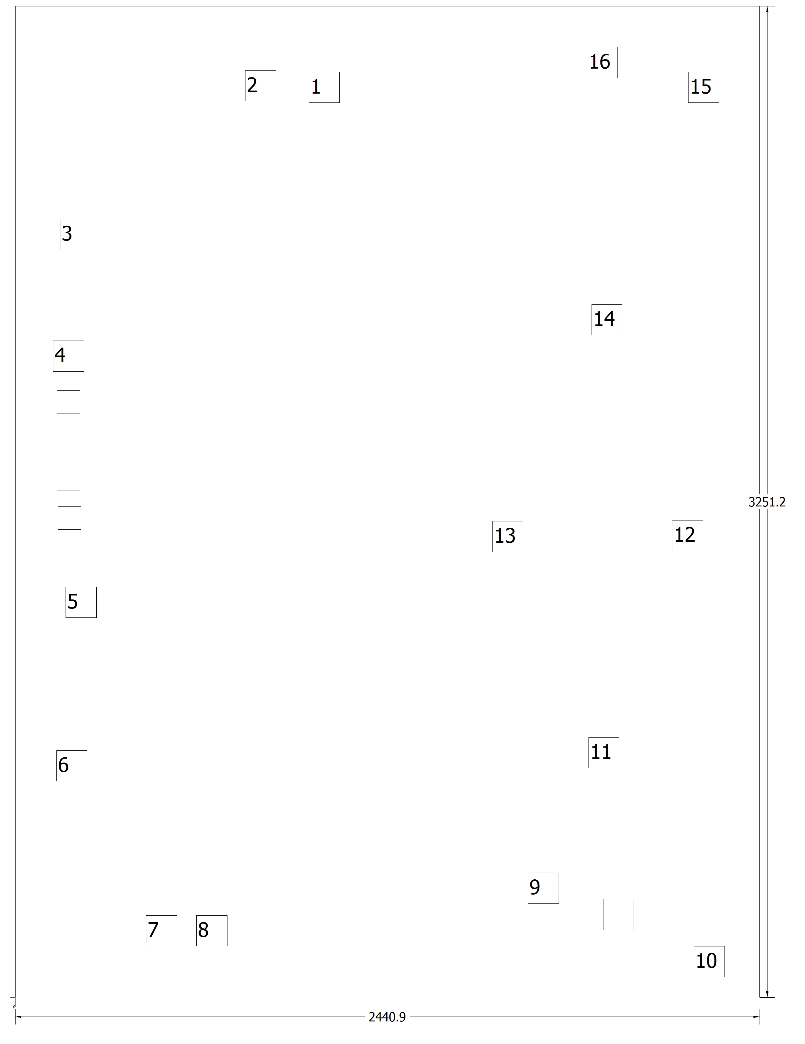
 Figure 5-2 UC1825B-SP Bare Die Pin Number
Locations
Figure 5-2 UC1825B-SP Bare Die Pin Number
LocationsTable 5-3 Bond Pad Coordinates in
Microns
| DESCRIPTION | PAD NUMBER | X MIN | Y MIN | X MAX | Y MAX |
|---|---|---|---|---|---|
|
INV |
1 |
962.66 |
2933.7 |
1064.26 |
3035.3 |
|
NI |
2 |
754.38 |
2938.78 |
855.98 |
3040.38 |
|
EAOUT |
3 |
147.32 |
2451.1 |
248.92 |
2552.7 |
|
CLK |
4 |
124.46 |
2052.32 |
226.06 |
2153.92 |
|
RT |
9 |
165.1 |
1244.6 |
266.7 |
1346.2 |
|
CT |
10 |
134.62 |
708.66 |
236.22 |
810.26 |
|
RAMP |
11 |
429.26 |
167.64 |
530.86 |
269.24 |
|
SS |
12 |
594.36 |
167.64 |
695.96 |
269.24 |
|
ILIM/SD |
13 |
1681.48 |
307.34 |
1783.08 |
408.94 |
|
GND |
15 |
2225.04 |
66.04 |
2326.64 |
167.64 |
|
OUTA |
16 |
1879.6 |
751.84 |
1981.2 |
853.44 |
|
PGND |
17 |
2153.92 |
1463.04 |
2255.52 |
1564.64 |
|
VC |
18 |
1564.64 |
1460.5 |
1666.24 |
1562.1 |
|
OUTB |
19 |
1889.76 |
2171.7 |
1991.36 |
2273.3 |
|
VCC |
20 |
2207.26 |
2933.7 |
2308.86 |
3035.3 |
|
RAMP |
21 |
1874.52 |
3014.98 |
1976.12 |
3116.58 |