SLUS872E January 2009 – February 2019 UC1842A-SP , UC1844A-SP
PRODUCTION DATA.
- 1 Features
- 2 Applications
- 3 Description
- 4 Revision History
- 5 Device Comparison Table
- 6 Pin Configuration and Functions
- 7 Specifications
- 8 Detailed Description
- 9 Application and Implementation
- 10Power Supply Recommendations
- 11Layout
- 12Device and Documentation Support
- 13Mechanical, Packaging, and Orderable Information
Package Options
Mechanical Data (Package|Pins)
- JG|8
Thermal pad, mechanical data (Package|Pins)
Orderable Information
10 Power Supply Recommendations
The devices are designed to operate from an input voltage supply range between 8 V and 40 V. This input supply should be well regulated. If the input supply is located more than a few inches from the UC184xA-SP converter, additional bulk capacitance may be required in addition to the ceramic bypass capacitors. A tantalum capacitor with a value of 47 µF is a typical choice; however, this may vary depending upon the output power being delivered.

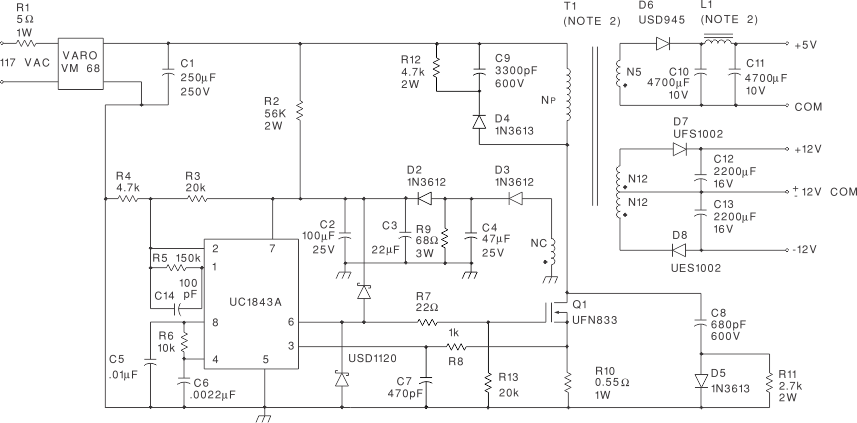
Power supply specifications:
Figure 25. Offline Flyback Regulator - Input voltage: 95 VAC to 130 VAC (50 Hz/60 Hz)
- Line isolation: 3750 V
- Switching frequency: 40 kHz
- Efficiency full load: 70%
- Output voltage:
- +5 V, ±5%; 1- to 4-A load, ripple voltage: 50 mVP-P max
- +12 V, ±3%; 0.1- to 0.3-A load, ripple voltage: 100 mVP-P max
- –12 V, ±3%; 0.1- to 0.3-A load, ripple voltage: 100 mVP-P max