SLUS336A June 1998 – December 2016 UC1854 , UC2854 , UC3854
PRODUCTION DATA.
- 1 Features
- 2 Applications
- 3 Description
- 4 Revision History
- 5 Device Comparison Table
- 6 Pin Configuration and Functions
- 7 Specifications
- 8 Detailed Description
- 9 Application and Implementation
- 10Power Supply Recommendations
- 11Layout
- 12Device and Documentation Support
- 13Mechanical, Packaging, and Orderable Information
Package Options
Refer to the PDF data sheet for device specific package drawings
Mechanical Data (Package|Pins)
- DW|16
- N|16
Thermal pad, mechanical data (Package|Pins)
- DW|16
Orderable Information
7 Specifications
7.1 Absolute Maximum Ratings
over operating free-air temperature range (unless otherwise noted)(1)(2)(3)(4)(5)| MIN | MAX | UNIT | ||
|---|---|---|---|---|
| Supply voltage | VCC | 35 | V | |
| Input Voltage | VSENSE, VRMS | 11 | V | |
| ISENSE, MULTOUT | 11 | |||
| PKLMT | 5 | |||
| Gate driver current Input current | 50% duty cycle | 1.5 | A | |
| Continuous | 0.5 | |||
| Input current | RSET, IAC, PKLMT, ENA | 10 | mA | |
| Power dissipation | 1 | W | ||
| Storage temperature, Tstg | –65 | 150 | °C | |
(1) Stresses beyond those listed under Absolute Maximum Ratings may cause permanent damage to the device. These are stress ratings only, which do not imply functional operation of the device at these or any other conditions beyond those indicated under Recommended Operating Conditions. Exposure to absolute-maximum-rated conditions for extended periods may affect device reliability.
(2) All voltages with respect to GND.
(3) All currents are positive into the specified terminal.
(4) ENA input is internally clamped to approximately 14 V.
(5) Consult Unitrode Integrated Circuits databook for information regarding thermal specifications and limitations.
7.2 ESD Ratings
| VALUE | UNIT | |||
|---|---|---|---|---|
| V(ESD) | Electrostatic discharge | Human-body model (HBM), per ANSI/ESDA/JEDEC JS-001(1) | ±2500 | V |
| Charged-device model (CDM), per JEDEC specification JESD22-C101(2) | ±1500 | |||
(1) JEDEC document JEP155 states that 500-V HBM allows safe manufacturing with a standard ESD control process.
(2) JEDEC document JEP157 states that 250-V CDM allows safe manufacturing with a standard ESD control process.
7.3 Recommended Operating Conditions
over operating free-air temperature range (unless otherwise noted)| MIN | MAX | UNIT | |||
|---|---|---|---|---|---|
| VCC | Supply voltage | 10 | 20 | ||
| TJ | Operating junction temperature | UC1854 | –55 | 125 | °C |
| UC2854 | –40 | 85 | |||
| UC3854 | 0 | 70 | |||
7.4 Thermal Information
| THERMAL METRIC(1) | UCx854 | UNIT | ||||
|---|---|---|---|---|---|---|
| DW (SOIC) | FN (PLCC) | J (CDIP) | N (PDIP) | |||
| 16 PINS | 20 PINS | 16 PINS | 16 PINS | |||
| RθJA | Junction-to-ambient thermal resistance | 71.5 | — | 25 | 40.8 | °C/W |
| RθJC(top) | Junction-to-case (top) thermal resistance | 32.7 | — | — | 26.8 | °C/W |
| RθJB | Junction-to-board thermal resistance | 36.3 | — | 5.5 | 20.9 | °C/W |
| ψJT | Junction-to-top characterization parameter | 6.8 | — | 2.1 | 10.9 | °C/W |
| ψJB | Junction-to-board characterization parameter | 35.8 | — | 5.4 | 20.7 | °C/W |
| RθJC(bot) | Junction-to-case (bottom) thermal resistance | — | — | 3.4 | — | °C/W |
(1) For more information about traditional and new thermal metrics, see the Semiconductor and IC Package Thermal Metricsapplication report.
7.5 Electrical Characteristics
Unless otherwise stated, VCC = 18 V, RSET = 15 kΩ to ground, CT = 1.5 nF to ground, VPKLMT = 1 V, VENA = 7.5 V,VRMS = 1.5 V, IAC = 100 µA, VISENSE = 0 V, VCAOUT = 3.5 V, VVAOUT = 5 V, VSENSE = 7.5 V, no load on SS, CAOUT, VAOUT, VREF, GTDRV, TA = TJ, TA = –55°C to 125°C for the UC1854, TA = –40°C to 85°C for the UC2854,
and TA = 0°C to 70°C for the UC3854.
| PARAMETER | TEST CONDITIONS | MIN | TYP | MAX | UNIT | |
|---|---|---|---|---|---|---|
| OVERALL | ||||||
| Supply current, OFF | VENA = 0 V | 1.5 | 2 | mA | ||
| Supply current, ON | 10 | 16 | mA | |||
| VCC turn-on threshold | 14.5 | 16 | 17.5 | V | ||
| VCC turn-off threshold | 9 | 10 | 11 | V | ||
| ENA threshold, rising | 2.4 | 2.55 | 2.7 | V | ||
| ENA threshold hysteresis | 0.2 | 0.25 | 0.3 | V | ||
| ENA input current | VENA = 0 V | –5 | –0.2 | 5 | µA | |
| VRMS input current | VRMS = 5 V | –1 | –0.01 | 1 | µA | |
| VOLTAGE AMPLIFIER | ||||||
| Voltage amplifier offset voltage | VVAOUT = 5 V | –8 | 8 | mV | ||
| VSENSE bias current | –500 | –25 | 500 | nA | ||
| Voltage amplifier gain | 70 | 100 | dB | |||
| Voltage amplifier output swing | 0.5 | 5.8 | V | |||
| Voltage amplifier short circuit current | VVAOUT = 0 V | –36 | –20 | –5 | mA | |
| SS current | VSS = 2.5 V | –20 | –14 | –6 | µA | |
| CURRENT AMPLIFIER | ||||||
| Current amplifier offset voltage | –4 | 4 | mV | |||
| ISENSE bias current | –500 | –120 | 500 | nA | ||
| Input range (ISENSE, MULTOUT) | –0.3 | 2.5 | V | |||
| Current amplifier gain | 80 | 110 | dB | |||
| Current amplifier output swing | 0.5 | 16 | V | |||
| Current amplifier short-circuit current | VCAOUT = 0 V | –36 | –20 | –5 | mA | |
| Current amplifier gain–bandwidth product | TA = 25°C(2) | 400 | 800 | kHz | ||
| REFERENCE | ||||||
| Reference output voltage | IREF = 0 mA, TA = 25°C | 7.4 | 7.5 | 7.6 | V | |
| Reference output voltage | IREF = 0 mA, over temperature | 7.35 | 7.5 | 7.65 | V | |
| VREF load regulation | –10 mA < IREF < 0 mA | –15 | 5 | 15 | mV | |
| VREF line regulation | 15 V < VCC < 35 V | –10 | 2 | 10 | mV | |
| VREF short circuit current | VREF = 0 V | –50 | –28 | –12 | mA | |
| MULTIPLIER | ||||||
| Multiplier out current IAC limited | IAC = 100 µA, RSET = 10 kΩ, VRMS = 1.25 V | –220 | –200 | –180 | µA | |
| Multiplier out current zero | IAC = 0 µA, RSET = 15 kΩ | –2 | –0.2 | –2 | µA | |
| Multiplier out current RSET limited | IAC = 450 µA, RSET = 15 kΩ, VRMS = 1 V, VVAOUT = 6 V |
–280 | –255 | –220 | µA | |
| Multiplier out current | IAC = 50 µA, VRMS = 2 V, VVAOUT = 4 V | –50 | –42 | –33 | µA | |
| Multiplier out current | IAC = 100 µA, VRMS = 2 V, VVAOUT = 2 V | –38 | –27 | –12 | µA | |
| Multiplier out current | IAC = 200 µA, VRMS = 2 V, VVAOUT = 4 V | –165 | –150 | –105 | µA | |
| Multiplier out current | IAC = 300 µA, VRMS = 1 V, VVAOUT = 2 V | –250 | –225 | –150 | µA | |
| Multiplier out current | IAC = 100 µA, VRMS = 1 V, VVAOUT = 2 V | –95 | –80 | –60 | µA | |
| Multiplier gain constant | See (1) | –1 | V | |||
| OSCILLATOR | ||||||
| Oscillator frequency | RSET = 15 kΩ | 46 | 55 | 62 | kHz | |
| Oscillator frequency | RSET = 8.2 kΩ | 86 | 102 | 118 | kHz | |
| CT ramp peak-to-valley amplitude | 4.9 | 5.4 | 5.9 | V | ||
| CT ramp valley voltage | 0.8 | 1.1 | 1.3 | V | ||
| GATE DRIVER (GTDRV) | ||||||
| Maximum gate driver output voltage | 0-mA load on gate driver, 18 V < VCC < 35 V | 13 | 14.5 | 18 | V | |
| Gate driver output voltage high | –200-mA load on gate driver, VCC = 15 V | 12 | 12.8 | V | ||
| Gate driver output voltage low, OFF | VCC = 0 V, 50-mA load on gate driver | 0.9 | 1.5 | V | ||
| Gate driver output voltage low | 200-mA load on gate driver | 1 | 2.2 | V | ||
| Gate driver output voltage low | 10-mA load on gate driver | 0.1 | 0.4 | V | ||
| Peak Gate driver current | 10 nF from gate driver to GND | 1 | A | |||
| Gate driver rise and fall time | 1 nF from gate driver to GND | 35 | ns | |||
| Gate driver maximum duty cycle | VCAOUT = 7 V | 95% | ||||
| CURRENT LIMIT | ||||||
| PKLMT offset voltage | –10 | 10 | mV | |||
| PKLMT input current | VPKLMT = –0.1 V | –200 | –100 | µA | ||
| PKLMT to gate driver delay | VPKLMT falling from 50 to –50 mV | 175 | ns | |||
(1) Multiplier gain constant (k) is defined by: 

(2) Specified by design. Not production tested.
7.6 Typical Characteristics
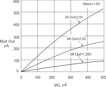
TA = TJ = 25°C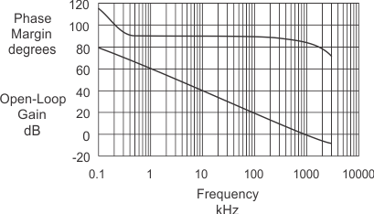 Figure 1. Current Amplifier Gain and Phase vs Frequency
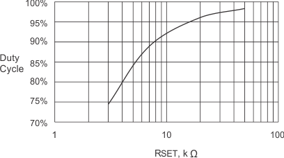
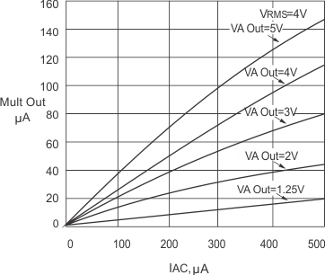
| VMULTOUT = 0 V |
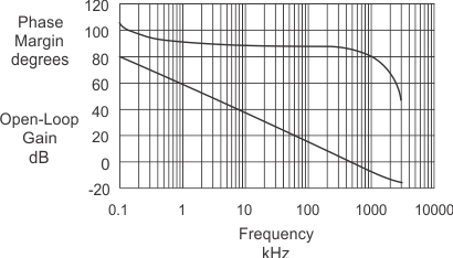 Figure 2. Voltage Amplifier Gain and Phase vs Frequency
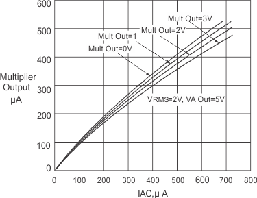 Figure 4. Multiplier Output vs Voltage On MULTOUT
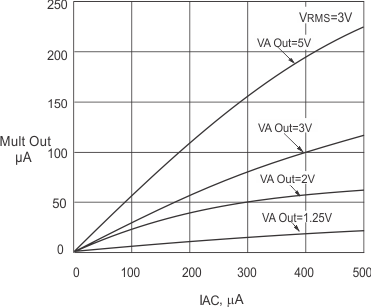
| VMULTOUT = 0 V |
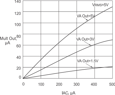
| VMULTOUT = 0 V |
