SLUSFC2 august   2023 UCC23113

PRODUCTION DATA  

  1.   1
  2. Features
  3. Applications
  4. Description
  5. Revision History
  6. Pin Configuration and Function
  7. Specifications
    1. 6.1 Absolute Maximum Ratings
    2. 6.2 ESD Ratings
    3. 6.3 Recommended Operating Conditions
    4. 6.4 Thermal Information
    5. 6.5 Power Ratings
    6. 6.6 Insulation Specifications
    7. 6.7 Electrical Characteristics
    8. 6.8 Switching Characteristics
    9. 6.9 Typical Characteristics
  8. Parameter Measurement Information
    1. 7.1 Propagation Delay, Rise Time and Fall Time
    2. 7.2 IOH and IOL testing
    3. 7.3 CMTI Testing
  9. Detailed Description
    1. 8.1 Overview
    2. 8.2 Functional Block Diagram
    3. 8.3 Feature Description
      1. 8.3.1 Power Supply
      2. 8.3.2 Input Stage
      3. 8.3.3 Output Stage
      4. 8.3.4 Protection Features
        1. 8.3.4.1 Undervoltage Lockout (UVLO)
        2. 8.3.4.2 Active Pulldown
        3. 8.3.4.3 Short-Circuit Clamping
    4. 8.4 Device Functional Modes
      1. 8.4.1 ESD Structure
  10. Application and Implementation
    1. 9.1 Application Information
    2. 9.2 Typical Application
      1. 9.2.1 Design Requirements
      2. 9.2.2 Detailed Design Procedure
        1. 9.2.2.1 Selecting the Input Resistor
        2. 9.2.2.2 Gate Driver Output Resistor
        3. 9.2.2.3 Estimate Gate-Driver Power Loss
        4. 9.2.2.4 Estimating Junction Temperature
        5. 9.2.2.5 Selecting VDD Capacitor
  11. 10Power Supply Recommendations
  12. 11Layout
    1. 11.1 Layout Guidelines
    2. 11.2 Layout Example
    3. 11.3 PCB Material
  13. 12Device and Documentation Support
    1. 12.1 Device Support
      1. 12.1.1 Third-Party Products Disclaimer
      2. 12.1.2 Development Support
    2. 12.2 Documentation Support
      1. 12.2.1 Related Documentation
    3. 12.3 Receiving Notification of Documentation Updates
    4. 12.4 Support Resources
    5. 12.5 Trademarks
    6. 12.6 Electrostatic Discharge Caution
    7. 12.7 Glossary
  14. 13Mechanical, Packaging, and Orderable Information

Package Options

Mechanical Data (Package|Pins)
Thermal pad, mechanical data (Package|Pins)
Orderable Information

CMTI Testing

Figure 7-3 is the simplified diagram of the CMTI testing. Common mode voltage is set to 1500V. The test is performed with IF = 10mA (VOUT= High) and IF = 0mA (VOUT = LOW). The diagram also shows the fail criteria for both cases. During the application on the CMTI pulse with IF = 10mA, if VOUT drops from VDD to ½VDD it is considered as a failure. With IF= 0mA, if VOUT rises above 1V, it is considered as a failure.
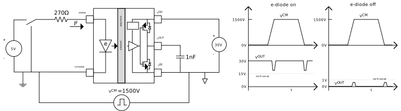
GUID-20230830-SS0I-LDPP-SDJQ-RZC7RJWMPN5T-low.svg Figure 7-3 CMTI Test Circuit for UCC23113