SLUSCM5A August 2017 – February 2018 UCC24612
PRODUCTION DATA.
- 1 Features
- 2 Applications
- 3 Description
- 4 Revision History
- 5 Pin Configuration and Functions
- 6 Specifications
- 7 Detailed Description
- 8 Application and Implementation
- 9 Power Supply Recommendations
- 10PCB Layout
- 11Device and Documentation Support
- 12Mechanical, Packaging, and Orderable Information
Package Options
Mechanical Data (Package|Pins)
- DBV|5
Thermal pad, mechanical data (Package|Pins)
Orderable Information
8.2.2.4 High-Side Operation
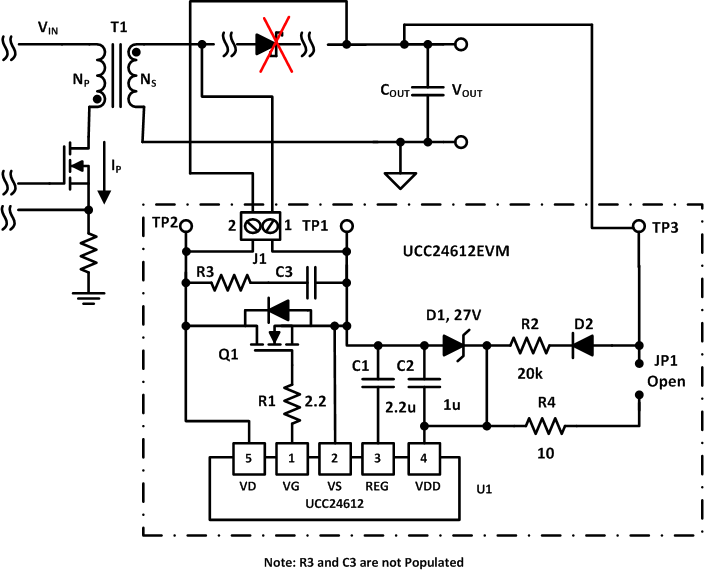
To use the UCC24612EVM to replace a high-side rectifier requires removing jumper JP1 and connecting the EVM as shown in Figure 23. Please note that the EVM comes with a default VDD filtering resistor (R2) of 20 kΩ. However, resistor R2 needs to be adjusted based on your individual application.
 Figure 23. UCC24612-1EVM Used in High-Side Rectifier Application
 If the magnitude of the voltage from TP2 to TP1 is less than 28 V, remove R2 that is populated on the EVM ( 20 kΩ) and set R2 to 0 to 10 ohms and remove 27-V Zener diode D1 from the board.
If TP2 to TP1 is greater than 28 V use resistor R2 to setup an averaging filter to lower the DC voltage applied to VDD.
The RC filter formed by C2 and R2 should set the filter pole frequency to one-hundredth of the converter's maximum switching frequency. In this example the converter's maximum switching frequency (fSW) is 85 kHz. Note that the switching frequency will vary based on design and preference.

When the RC filter circuit is used, it is recommended that the VDD voltage should be between 4 V to 28 V to provide enough energy and voltage to the gate driver. This range can be determined in a fixed frequency Flyback converter with the following equations. DMAX is the maximum duty cycle of the converter and DMIN is the minimum duty cycle of the converter. NP is the Flyback transformer (T1) primary number of turns and NS is the transformer secondary number of turns. Please refer to Figure 23 for details.
Maximum VDD voltage (VVDD(MAX)):

Minimum VDD voltage (VVDD(MIN)):
