SLUSDU4A December 2020 – May 2022 UCC27289
PRODUCTION DATA
- 1 Features
- 2 Applications
- 3 Description
- 4 Revision History
- 5 Pin Configuration and Functions
- 6 Specifications
- 7 Detailed Description
- 8 Application and Implementation
- 9 Power Supply Recommendations
- 10Layout
- 11Device and Documentation Support
- 12Mechanical, Packaging, and Orderable Information
Package Options
Mechanical Data (Package|Pins)
Thermal pad, mechanical data (Package|Pins)
- DRC|10
Orderable Information
8.2.2.3 Estimate Driver Power Losses
The total power loss in gate driver device such as the UCC27289 is the summation of the power loss in different functional blocks of the gate driver device. These power loss components are explained in this section.
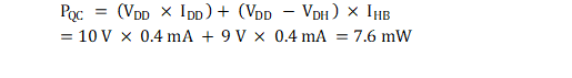
- Equation 4 describes how quiescent currents (IDD and IHB) affect the static power losses, PQC.
Equation 4.
it is not shown here, but for more conservative approximation, add no load operating current, IDDO and IHBO in above equation.
- Equation 5 shows how high-side to low-side leakage current (IHBS) affects level-shifter losses (PIHBS).
Equation 5.

where
- D is the high-side MOSFET duty cycle
- VHB is the sum of input voltage and voltage across bootstrap capacitor.
- Equation 6 shows how MOSFETs gate charge (QG) affects the dynamic losses, PQG.
Equation 6.

where
- QG is the total MOSFET gate charge
- fSW is the switching frequency
- RGD_R is the average value of pullup and pulldown resistor
- RGATE is the external gate drive resistor
- RGFET(int) is the power MOSFETs internal gate resistor
Assume there is no external gate resistor in this example. The average value of maximum pull-up and pull down resistance of the driver output section is approximately 4 Ω. Substitute the application values to calculate the dynamic loss due to gate charge, which is 230 mW here.
- Equation 7 shows how parasitic level-shifter charge (QP) on each switching cycle affects dynamic losses, (PLS) during high-side switching.
Equation 7.

For this example and simplicity, it is assumed that value of parasitic charge QP is 1 nC. Substituting values results in 25.5 mW as level shifter dynamic loss. This estimate is very high for level shifter dynamic losses.
The sum of all the losses is 265.22 mW as a total gate driver loss. As shown in this example, in most applications the dynamic loss due to gate charge dominates the total power loss in gate driver device. For gate drivers that include bootstrap diode, one should also estimate losses in bootstrap diode. Diode forward conduction loss is computed as product of average forward voltage drop and average forward current.
Equation 8 estimates the maximum allowable power loss of the device for a given ambient temperature.

where
- PMAX is the maximum allowed power dissipation in the gate driver device
- TJ is the recommended maximum operating junction temperature
- TA is hte ambient temperature of the gate driver device
- RθJA is the junction-to-ambient thermal resistance
To better estimate the junction temperature of the gate driver device in the application, it is recommended to first accurately measure the case temperature and then determine the power dissipation in a given application. Then use ψJT to calculate junction temperature. After estimating junction temperature and measuring ambient temperature in the application, calculate θJA(effective). Then, if design parameters (such as the value of an external gate resistor or power MOSFET) change during the development of the project, use θJA(effective) to estimate how these changes affect junction temperature of the gate driver device.
The Thermal Information table summarizes the thermal metrics for the driver package. For detailed information regarding the thermal information table, please refer to the Semiconductor and Device Package Thermal Metrics application report.