SLUSEY2A june   2023  – august 2023 UCC27311A-Q1

ADVANCE INFORMATION  

  1.   1
  2. Features
  3. Applications
  4. Description
  5. Revision History
  6. Description (continued)
  7. Pin Configuration and Functions
  8. Specifications
    1. 7.1 Absolute Maximum Ratings
    2. 7.2 ESD Ratings
    3. 7.3 Recommended Operating Conditions
    4. 7.4 Thermal Information
    5. 7.5 Electrical Characteristics
    6. 7.6 Switching Characteristics
    7. 7.7 Timing Diagrams
  9. Detailed Description
    1. 8.1 Overview
    2. 8.2 Functional Block Diagram
    3. 8.3 Feature Description
      1. 8.3.1 Input Stages
      2. 8.3.2 Enable
      3. 8.3.3 Undervoltage Lockout (UVLO)
      4. 8.3.4 Level Shifter
      5. 8.3.5 Boot Diode
      6. 8.3.6 Output Stages
      7. 8.3.7 Negative Voltage Transients
    4. 8.4 Device Functional Modes
  10. Application and Implementation
    1. 9.1 Application Information
    2. 9.2 Typical Application
      1. 9.2.1 Design Requirements
      2. 9.2.2 Detailed Design Procedure
        1. 9.2.2.1 Input Threshold Type
        2. 9.2.2.2 VDD Bias Supply Voltage
        3. 9.2.2.3 Peak Source and Sink Currents
        4. 9.2.2.4 Propagation Delay
        5. 9.2.2.5 Power Dissipation
  11. 10Power Supply Recommendations
  12. 11Layout
    1. 11.1 Layout Guidelines
    2. 11.2 Layout Example
    3. 11.3 Thermal Considerations
  13. 12Device and Documentation Support
    1. 12.1 Device Support
      1. 12.1.1 Third-Party Products Disclaimer
    2. 12.2 Documentation Support
      1. 12.2.1 Related Documentation
    3. 12.3 Receiving Notification of Documentation Updates
    4. 12.4 Support Resources
    5. 12.5 Trademarks
    6. 12.6 Electrostatic Discharge Caution
    7. 12.7 Glossary
  14. 13Mechanical, Packaging, and Orderable Information
    1. 13.1 Package Option Addendum
      1.      55
    2. 13.2 Tape and Reel Information
    3. 13.3 Mechanical Data

Refer to the PDF data sheet for device specific package drawings

Mechanical Data (Package|Pins)
  • DRC|10
Thermal pad, mechanical data (Package|Pins)

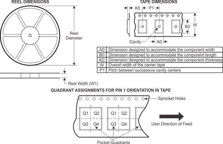
Tape and Reel Information

GUID-DCD52EFC-87A4-47A4-9D04-3D3EAC01766F-low.gif
Device Package
Type
Package Drawing Pins SPQ Reel
Diameter (mm)
Reel
Width W1 (mm)
A0
(mm)
B0
(mm)
K0
(mm)
P1
(mm)
W
(mm)
Pin1
Quadrant
PUCC27311AQDRCRQ1 VSON DRC 10 3000 330.0 12.4 3.3 3.3 1.1 8.0 12.0 Q2
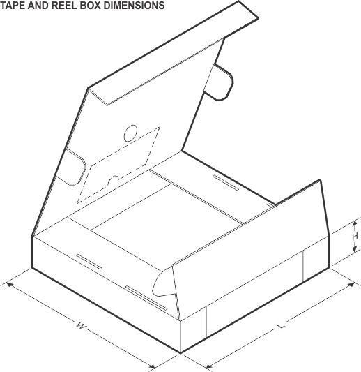
GUID-AC13D00E-1D4D-44B4-9306-767344F9384F-low.gif
Device Package Type Package Drawing Pins SPQ Length (mm) Width (mm) Height (mm)
PUCC27311AQDRCRQ1 VSON DRC 10 3000 367.0 367.0 35