SLUSEW3 October   2023 UCC27332-Q1

PRODUCTION DATA  

  1.   1
  2. Features
  3. Applications
  4. Description
  5. Revision History
  6. Pin Configuration and Functions
  7. Specifications
    1. 6.1 Absolute Maximum Ratings
    2. 6.2 ESD Ratings
    3. 6.3 Recommended Operating Conditions
    4. 6.4 Thermal Information
    5. 6.5 Electrical Characteristics
    6. 6.6 Switching Characteristics
    7. 6.7 Timing Diagrams
    8. 6.8 Typical Characteristics
  8. Detailed Description
    1. 7.1 Overview
    2. 7.2 Functional Block Diagram
    3. 7.3 Feature Description
      1. 7.3.1 VDD Power On Reset
      2. 7.3.2 Input Stage
      3. 7.3.3 Enable Function
      4. 7.3.4 Output Stage
    4. 7.4 Device Functional Modes
  9. Applications and Implementation
    1. 8.1 Application Information
    2. 8.2 Typical Application
      1. 8.2.1 Driving MOSFET
        1. 8.2.1.1 Design Requirements
        2. 8.2.1.2 Detailed Design Procedure
          1. 8.2.1.2.1 Input-to-Output Configuration
          2. 8.2.1.2.2 Input Threshold Type
          3. 8.2.1.2.3 VDD Bias Supply Voltage
          4. 8.2.1.2.4 Peak Source and Sink Currents
          5. 8.2.1.2.5 Enable and Disable Function
          6. 8.2.1.2.6 Propagation Delay and Minimum Input Pulse Width
          7. 8.2.1.2.7 Power Dissipation
        3. 8.2.1.3 Application Curves
    3. 8.3 Power Supply Recommendations
    4. 8.4 Layout
      1. 8.4.1 Layout Guidelines
      2. 8.4.2 Layout Example
      3. 8.4.3 Thermal Consideration
  10. Device and Documentation Support
    1. 9.1 Third-Party Products Disclaimer
    2. 9.2 Receiving Notification of Documentation Updates
    3. 9.3 Support Resources
    4. 9.4 Trademarks
    5. 9.5 Electrostatic Discharge Caution
    6. 9.6 Glossary
  11. 10Mechanical, Packaging, and Orderable Information

Package Options

Mechanical Data (Package|Pins)
Thermal pad, mechanical data (Package|Pins)
Orderable Information

VDD Power On Reset

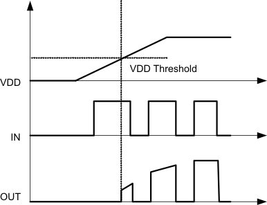
The UCC27332-Q1 device offers an power on reset lockout threshold of 3.0 V (rising). The device's hysteresis range helps to avoid any chattering due to the presence of noise on the bias supply. 0.3 V of typical POR hysteresis is expected for 4-V devices. There is no significant driver output turnon delay due to the POR feature. The POR turn-off delay is also minimized as much as possible. The POR delay is designed to minimize chattering that may occur due to very fast transients that may appear on VDD. When the bias supply is below POR thresholds, the outputs are held actively low irrespective of the state of input pins and enable pin. The device accepts a wide range of slew rates on its VDD pin.
GUID-40B40313-2FDE-4C67-B069-E25375659FC9-low.gifFigure 7-1 Power Up