SLUSAW9F February 2012 – November 2014 UCC27511 , UCC27512
PRODUCTION DATA.
- 1 Features
- 2 Applications
- 3 Description
- 4 Revision History
- 5 Description (Continued)
- 6 UCC2751x Product Family
- 7 Pin Configuration and Functions
- 8 Specifications
- 9 Detailed Description
- 10Application and Implementation
- 11Power Supply Recommendations
- 12Layout
- 13Device and Documentation Support
- 14Mechanical, Packaging, and Orderable Information
Package Options
Mechanical Data (Package|Pins)
- DRS|6
Thermal pad, mechanical data (Package|Pins)
- DRS|6
Orderable Information
10 Application and Implementation
NOTE
Information in the following applications sections is not part of the TI component specification, and TI does not warrant its accuracy or completeness. TI’s customers are responsible for determining suitability of components for their purposes. Customers should validate and test their design implementation to confirm system functionality.
10.1 Application Information
High-current gate-driver devices are required in switching-power applications for a variety of reasons. In order to effect fast switching of power devices and reduce associated switching power losses, a powerful gate driver employs between the PWM output of controllers and the gates of the power-semiconductor devices. Further, gate drivers are indispensable when having the PWM controller directly drive the gates of the switching devices is impossible. With advent of digital power, this situation will be often encountered since the PWM signal from the digital controller is often a 3.3-V logic signal which is not capable of effectively turning on a power switch. A level-shifting circuitry is needed to boost the 3.3-V signal to the gate-drive voltage (such as 12 V) in order to fully turn on the power device and minimize conduction losses. Traditional buffer drive circuits based on NPN/PNP bipolar transistors in totem-pole arrangement, being emitter follower configurations, prove inadequate with digital power since they lack level-shifting capability. Gate drivers effectively combine both the level-shifting and buffer-drive functions. Gate drivers also find other needs such as minimizing the effect of high-frequency switching noise by locating the high-current driver physically close to the power switch, driving gate-drive transformers and controlling floating power-device gates, reducing power dissipation and thermal stress in controllers by moving gate charge power losses into itself. Finally, emerging wide band-gap power device technologies such as GaN based switches, which are capable of supporting very high switching frequency operation, are driving very special requirements in terms of gate drive capability. These requirements include operation at low VDD voltages (5 V or lower), low propagation delays and availability in compact, low-inductance packages with good thermal capability. In summary gate-driver devices are extremely important components in switching power combining benefits of high-performance low-cost component count and board-space reduction and simplified system design.
10.2 Typical Application
Typical application diagrams of UCC27511 and UCC27512 devices are shown below illustrating use in non-inverting and inverting driver configurations. The UCC27511 device features a unique split output configuration where the gate-drive current is sourced through OUTH pin and sunk through OUTL pin. This unique pin arrangement allows user to apply independent turn-on and turn-off resistors to the OUTH and OUTL pins respectively and easily control the turn-on and turn-off switching dV/dt. This pin arrangement, along with the low pulldown impedance of the output driver stage, is especially handy in applications where a high C x dV/dt Miller turnon immunity is needed (such as with GaN power switches, SR MOSFETs, and so forth) and OUTL pin can be directly tied to the gate of the power device.
 Figure 25. Using Noninverting Input (IN– Is Grounded to Enable Output)
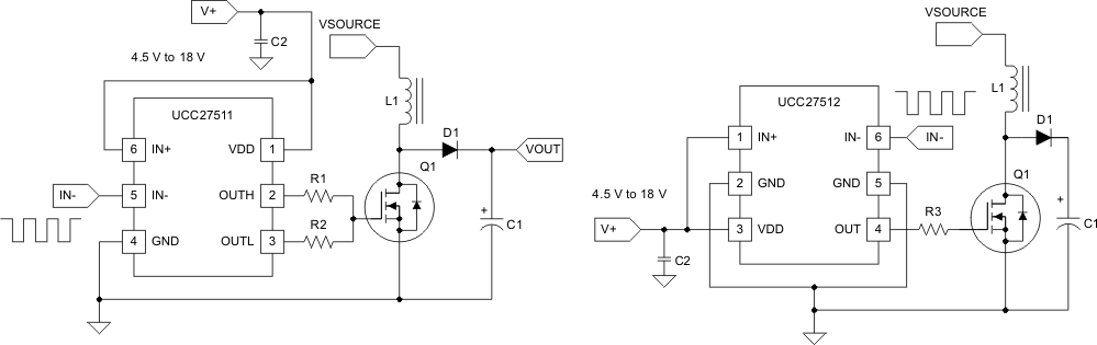 Figure 26. Using Inverting Input (IN+ Is Tied to VDD Enable Output)
NOTE
The UCC27512 features two ground pins, pin 2 and pin 5. TI recommends tying both pins together using PCB trace as close as possible to the device.
10.2.1 Design Requirements
When selecting the proper gate driver device for an end application, some design considerations must be evaluated first in order to make the most appropriate selection. Among these considerations are input-to-output configuration, the input threshold type, bias supply voltage levels, peak source and sink currents, availability of independent enable and disable functions, propagation delay, power dissipation, and package type.
10.2.2 Detailed Design Procedure
10.2.2.1 Input-to-Output Logic
The design should specify which type of input-to-output configuration should be used. If turning on the power MOSFET or IGBT when the input signal is in high state is preferred, then the non-inverting configuration must be selected. If turning off the power MOSFET or IGBT when the input signal is in high state is preferred, the inverting configuration must be chosen. The UCC27511 and UCC27512 devices can be configured in either an inverting or noninverting input-to-output configuration using the IN– or IN+ pins respectively. To configure the device for use in inverting mode, tie the IN+ pin to VDD and apply the input signal to the IN– pin. For the noninverting configuration, tie the IN– pin to GND and apply the input signal to the IN+ pin.
10.2.2.2 Input Threshold Type
The type of Input voltage threshold determines the type of controller that can be used with the gate driver device. The UCC27511 and UCC27512 devices feature a TTL and CMOS-compatible input threshold logic, with wide hysteresis. The threshold voltage levels are low voltage and independent of the VDD supply voltage, which allows compatibility with both logic-level input signals from microcontrollers as well as higher-voltage input signals from analog controllers. See the Electrical Characteristics table for the actual input threshold voltage levels and hysteresis specifications for the UCC27511 and UCC27512 devices.
10.2.2.3 VDD Bias Supply Voltage
The bias supply voltage to be applied to the VDD pin of the device should never exceed the values listed in the Recommended Operating Conditions table. However, different power switches demand different voltage levels to be applied at the gate terminals for effective turnon and turnoff. With certain power switches, a positive gate voltage may be required for turnon and a negative gate voltage may be required for turnoff, in which case the VDD bias supply equals the voltage differential. With a wide operating range from 4.5 V to 18 V, the UCC27511 and UCC27512 devices can be used to drive a variety of power switches, such as Si MOSFETs (for example, VGS = 4.5 V, 10 V, 12 V), IGBTs (VGE = 15 V, 18 V), and wide-bandgap power semiconductors (such as GaN, certain types of which allow no higher than 6 V to be applied to the gate terminals).
10.2.2.4 Peak Source and Sink Currents
Generally, the switching speed of the power switch during turnon and turnoff should be as fast as possible in order to minimize switching power losses. The gate driver device must be able to provide the required peak current for achieving the targeted switching speeds for the targeted power MOSFET.
Using the example of a power MOSFET, the system requirement for the switching speed is typically described in terms of the slew rate of the drain-to-source voltage of the power MOSFET (such as dVDS/dt). For example, the system requirement might state that a SPP20N60C3 power MOSFET must be turned-on with a dVDS/dt of 20 V/ns or higher under a DC bus voltage of 400 V in a continuous-conduction-mode (CCM) boost PFC-converter application. This type of application is an inductive hard-switching application and reducing switching power losses is critical. This requirement means that the entire drain-to-source voltage swing during power MOSFET turn-on event (from 400 V in the OFF state to VDS(on) in on state) must be completed in approximately 20 ns or less. When the drain-to-source voltage swing occurs, the Miller charge of the power MOSFET (QGD parameter in SPP20N60C3 power MOSFET data sheet = 33 nC typical) is supplied by the peak current of gate driver. According to power MOSFET inductive switching mechanism, the gate-to-source voltage of the power MOSFET at this time is the Miller plateau voltage, which is typically a few volts higher than the threshold voltage of the power MOSFET, VGS(TH).
In order to achieve the targeted dVDS/dt, the gate driver must be capable of providing the QGD charge in 20 ns or less. In other words a peak current of 1.65 A (= 33 nC / 20 ns) or higher must be provided by the gate driver. The UCC27511 and UCC27512 gate driver is capable of providing 4-A peak sourcing current which clearly exceeds the design requirement and has the capability to meet the switching speed needed. The 2.4x overdrive capability provides an extra margin against part-to-part variations in the QGD parameter of the power MOSFET along with additional flexibility to insert external gate resistors and fine tune the switching speed for efficiency versus EMI optimizations.
However, in practical designs the parasitic trace inductance in the gate drive circuit of the PCB will have a definitive role to play on the power MOSFET switching speed. The effect of this trace inductance is to limit the dI/dt of the output current pulse of the gate driver. In order to illustrate this, consider output current pulse waveform from the gate driver to be approximated to a triangular profile, where the area under the triangle (½ × IPEAK × time) would equal the total gate charge of the power MOSFET (QG parameter in SPP20N60C3 power MOSFET datasheet = 87 nC typical). If the parasitic trace inductance limits the dI/dt then a situation may occur in which the full peak current capability of the gate driver is not fully achieved in the time required to deliver the QG required for the power MOSFET switching. In other words the time parameter in the equation would dominate and the IPEAK value of the current pulse would be much less than the true peak current capability of the device, while the required QG is still delivered. Because of this, the desired switching speed may not be realized, even when theoretical calculations indicate the gate driver is capable of achieving the targeted switching speed. Thus, placing the gate driver device very close to the power MOSFET and designing a tight gate drive-loop with minimal PCB trace inductance is important to realize the full peak-current capability of the gate driver.
10.2.2.5 Enable and Disable Function
Certain applications demand independent control of the output state of the driver without involving the input signal. A pin which offers an enable and disable function achieves this requirement. The UCC27511 and UCC27512 devices offer 2 input pins, IN+ and IN–, both of which control the state of the output as listed in Table 3. Based on whether an inverting or noninverting input signal is provided to the driver, the appropriate input pin can be selected as the primary input for controlling the gate driver. The other unused input pin can be conveniently used for the enable and disable functionality. If the design does not require an enable function, the unused input pin can be tied to either the VDD pin (in case IN+ is the unused pin), or GND (in case IN– is unused pin) in order to ensure it does not affect the output status.
10.2.2.6 Propagation Delay
The acceptable propagation delay from the gate driver is dependent on the switching frequency at which it is used and the acceptable level of pulse distortion to the system. The UCC27511 and UCC27512 devices feature industry best-in-class 13-ns (typical) propagation delays which ensures very little pulse distortion and allows operation at very high-frequencies. See the table for the propagation and switching characteristics of the UCC27511 and UCC27512 devices.
10.2.2.7 Thermal Information
The useful range of a driver is greatly affected by the drive-power requirements of the load and the thermal characteristics of the package. In order for a gate driver to be useful over a particular temperature range the package must allow for the efficient removal of the heat produced while keeping the junction temperature within rated limits. The thermal metrics for the driver package is listed in the table. For detailed information regarding the table, please refer to the Application Note from Texas Instruments entitled IC Package Thermal Metrics (SPRA953).
The UCC27511 device is offered in a SOT-23, 6-pin package (DBV). The section lists the thermal performance metrics related to SOT-23 package. The ψJT and ψJB metrics are used when estimating the die temperature during actual application measurements.
Heat removal occurs primarily through the leads of the device and the PCB traces connected to the leads.
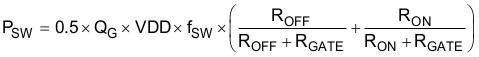
10.2.2.8 Power Dissipation
Power dissipation of the gate driver has two portions as shown in Equation 1.

The DC portion of the power dissipation is PDC = IQ x VDD where IQ is the quiescent current for the driver. The quiescent current is the current consumed by the device to bias all internal circuits such as input stage, reference voltage, logic circuits, protections, and also any current associated with switching of internal devices when the driver output changes state (such as charging and discharging of parasitic capacitances, parasitic shoot-through, and so forth). The UCC27511 and UCC27512 features very low quiescent currents (less than 1 mA, refer Figure 7) and contains internal logic to eliminate any shoot-through in the output driver stage. Thus the effect of the PDC on the total power dissipation within the gate driver can be safely assumed to be negligible.
The power dissipated in the gate-driver package during switching (PSW) depends on the following factors:
- Gate charge required of the power device (usually a function of the drive voltage VG, which is very close to input bias supply voltage VDD due to low VOH drop-out).
- Switching frequency.
- Use of external gate resistors.
When a driver device is tested with a discrete, capacitive load calculating the power that is required from the bias supply is fairly simple. The energy that must be transferred from the bias supply to charge the capacitor is given by Equation 2.
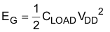
where
- CLOAD is load capacitor
- VDD is bias voltage feeding the driver
There is an equal amount of energy dissipated when the capacitor is charged. This leads to a total power loss given by Equation 3.
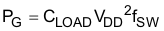
where
- ƒSW is the switching frequency
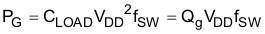
The switching load presented by a power MOSFET/IGBT is converted to an equivalent capacitance by examining the gate charge required to switch the device. This gate charge includes the effects of the input capacitance plus the added charge needed to swing the drain voltage of the power device as it switches between the ON and OFF states. Most manufacturers provide specifications of typical and maximum gate charge, in nC, to switch the device under specified conditions. Using the gate charge Qg, determine the power that must be dissipated when charging a capacitor which is calculated using the equation, QG = CLOAD x VDD, to provide Equation 4 for power.
This power PG is dissipated in the resistive elements of the circuit when the MOSFET/IGBT is being turned on or off. Half of the total power is dissipated when the load capacitor is charged during turnon, and the other half is dissipated when the load capacitor is discharged during turnoff. When no external gate resistor is employed between the driver and MOSFET/IGBT, this power is completely dissipated inside the driver package. With the use of external gate-drive resistors, the power dissipation is shared between the internal resistance of driver and external gate resistor in accordance to the ratio of the resistances (more power dissipated in the higher resistance component). Based on this simplified analysis, the driver power dissipation during switching is calculated in Equation 5.