SLUSDW0B May 2020 – May 2020 UCC28065
PRODUCTION DATA.
- 1 Features
- 2 Applications
- 3 Description
- 4 Revision History
- 5 Description (Continued)
- 6 Pin Configuration and Functions
- 7 Specifications
-
8 Detailed Description
- 8.1 Overview
- 8.2 Functional Block Diagram
- 8.3
Feature Description
- 8.3.1 Principles of Operation
- 8.3.2 Natural Interleaving
- 8.3.3 On-Time Control, Maximum Frequency Limiting, Restart Timer and Input Voltage Feed-Forward compensation
- 8.3.4 Zero-Current Detection and Valley Switching
- 8.3.5 Phase Management and Light-Load Operation
- 8.3.6 Burst Mode Operation
- 8.3.7 External Disable
- 8.3.8 Improved Error Amplifier
- 8.3.9 Soft Start
- 8.3.10 Brownout Protection
- 8.3.11 Line Dropout Detection
- 8.3.12 VREF
- 8.3.13 VCC
- 8.3.14
System Level Protections
- 8.3.14.1 Failsafe OVP - Output Over-voltage Protection
- 8.3.14.2 Overcurrent Protection
- 8.3.14.3 Open-Loop Protection
- 8.3.14.4 VCC Undervoltage Lock-Out (UVLO) Protection
- 8.3.14.5 Phase-Fail Protection
- 8.3.14.6 CS - Open, TSET - Open and Short Protection
- 8.3.14.7 Thermal Shutdown Protection
- 8.3.14.8 Fault Logic Diagram
- 8.4 Device Functional Modes
-
9 Application and Implementation
- 9.1 Application Information
- 9.2
Typical Application
- 9.2.1 Design Requirements
- 9.2.2
Detailed Design Procedure
- 9.2.2.1 Inductor Selection
- 9.2.2.2 ZCD Resistor Selection RZA, RZB
- 9.2.2.3 HVSEN
- 9.2.2.4 Output Capacitor Selection
- 9.2.2.5 Selecting RS For Peak Current Limiting
- 9.2.2.6 Power Semiconductor Selection (Q1, Q2, D1, D2)
- 9.2.2.7 Brownout Protection
- 9.2.2.8 Converter Timing
- 9.2.2.9 Programming VOUT
- 9.2.2.10 Voltage Loop Compensation
- 9.2.3 Application Curves
- 10Power Supply Recommendations
- 11Layout
- 12Device and Documentation Support
- 13Mechanical, Packaging, and Orderable Information
Package Options
Mechanical Data (Package|Pins)
- D|16
Thermal pad, mechanical data (Package|Pins)
Orderable Information
8.3.9 Soft Start
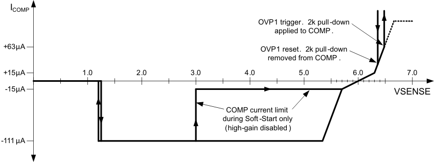
Soft-start is a process for boosting the output voltage of the PFC converter from the peak of the ac-line input voltage to the desired regulation voltage under controlled conditions. Instead of a dedicated soft-start pin, the UCC28065 uses the voltage error amplifier as a controlled current source to increase the PWM duty-cycle by way of increasing the COMP voltage. To avoid excessive start-up time-delay when the ac-line voltage is low, a higher current is applied until VSENSE exceeds 3 V at which point the current is reduced to minimize the tendency for excess COMP voltage at no-load start-up.
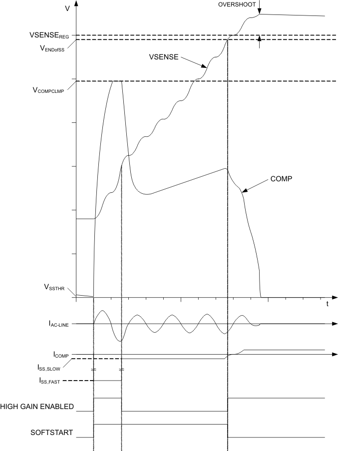
The PWM gradually ramps from zero on-time to normal on-time as the compensation capacitor from COMP to AGND charges from zero to near its final value. This process implements a soft-start, with timing set by the output current of the error amplifier and the value of the compensation capacitors. Soft-start ends when VSENSE pin voltage exceeds 95% of VSENSEreg. During soft-start the device will operate with both phases on and even if the COMP voltage is below the BRST pin voltage the device will not stop switching. In the event of a HVSEN failsafe OVP, brownout, external-disable, UVLO fault, or other protection faults, COMP is actively discharged and the UCC28065 will soft-start after the triggering event is cleared. Even if a fault event happens very briefly, the fault is latched into the soft-start state and soft-start is delayed until COMP is fully discharged to 20 mV and the fault is cleared. See Figure 26 for details on the COMP current. See Figure 27 which illustrates an example of typical system behavior during soft-start.

 Figure 27. Soft-Start Timing with System Behavior