SLUSBD8E February 2013 – December 2014 UCC28251
PRODUCTION DATA.
- 1 Features
- 2 Applications
- 3 Description
- 4 Revision History
- 5 Description (continued)
- 6 Pin Configuration and Functions
- 7 Specifications
-
8 Detailed Description
- 8.1 Overview
- 8.2 Functional Block Diagram
- 8.3
Feature Description
- 8.3.1 VDD (5/12)
- 8.3.2 VREF (Reference Generator) (20/7)
- 8.3.3 EN (Enable Pin) (18/5)
- 8.3.4 RT (Oscillator Frequency Set and Synchronization) (15/2)
- 8.3.5 SP (Synchronous Rectifier Turn-Off to Primary Output Turn-On Dead Time Programming) (13/19)
- 8.3.6 PS (Primary Output Turn-Off to Synchronous Rectifier Turn-On Dead Time Programming) (11/18)
- 8.3.7 RAMP/CS (PWM Ramp Input or Current Sense Input) (16/3)
- 8.3.8 REF/EA+ (1/8)
- 8.3.9 FB/EA- (2/9)
- 8.3.10 COMP (3/10)
- 8.3.11 VSENSE (14/1)
- 8.3.12 SS (Soft Start Programming Pin) (13/20)
- 8.3.13 ILIM (Current Limit for Cycle-by-Cycle Over-Current Protection) (17/4)
- 8.3.14 HICC (10/17)
- 8.3.15 OVP/OTP (19/6)
- 8.3.16 OUTA (9/16) and OUTB (8/15)
- 8.3.17 SRA (7/14) and SRB (6/13)
- 8.3.18 GND (4/11)
- 8.4 Device Functional Modes
-
9 Application and Implementation
- 9.1 Application Information
- 9.2
Typical Applications
- 9.2.1
Circuit Diagram in Design Example
- 9.2.1.1 Design Requirements
- 9.2.1.2
Detailed Design Procedure
- 9.2.1.2.1 Step 1: Power Stage Design
- 9.2.1.2.2 Step 2: Feedback Loop Design
- 9.2.1.2.3 Step 3: Programming The Device
- 9.2.1.2.4 Step 3-3: Determine Soft-Start Capacitance
- 9.2.1.2.5 Step 3-4: Determine Dead-Time Resistance
- 9.2.1.2.6 Step 3-5: Determine OCP Hiccup Off-Time Capacitance
- 9.2.1.2.7 Step 3-6: Determine Primary-Side OVP Resistance
- 9.2.1.2.8 Step 3-7: Select Capacitance for VDD and VREF
- 9.2.1.3 Application Curves
- 9.2.2 Secondary-Side Half-Bridge Controller With Synchronous Rectification
- 9.2.1
Circuit Diagram in Design Example
- 10Power Supply Recommendations
- 11Layout
- 12Device and Documentation Support
- 13Mechanical, Packaging, and Orderable Information
Package Options
Mechanical Data (Package|Pins)
Thermal pad, mechanical data (Package|Pins)
- RGP|20
Orderable Information
9 Application and Implementation
NOTE
Information in the following applications sections is not part of the TI component specification, and TI does not warrant its accuracy or completeness. TI’s customers are responsible for determining suitability of components for their purposes. Customers should validate and test their design implementation to confirm system functionality.
9.1 Application Information
The UCC28251 is a high performance PWM controller with advanced synchronous rectifier outputs and is ideally suited for regulated half-bridge, full-bridge and push-pull converters. A dedicated internal pre-biased start up control loop working in conjunction with a primary-side voltage loop achieves monotonic pre-biased start up for either primary-side or secondary-side control applications. The UCC28251 architecture allows either voltage mode or current mode control.
Input voltage feedforward can be implemented, allowing PWM ramp generator to improve the converter line transient response. Advanced cycle-by-cycle current limit achieves volt-second balancing even during fault conditions. The hiccup timer helps the system to stay within a safe operation range under over load conditions. With a multifunction OVP/OTP pin, combinations of input voltage protection, output voltage protection and over temperature protection can be implemented. The UCC28251 allows individual programming of dead time between primary-side switch and secondary-side SRs, in order to allow optimal power stage design. Dead time can also be reduced to zero, and this allows optimal system configuration considering the delays on the gate driver stage. The UCC28251 also provides complete system level protection functions, including UVLO, thermal shut down and over voltage, over current protection.
9.1.1 Error Amplifier and PWM Generation
The UCC28251 includes a high performance internal error amplifier with low input offset, high source/sink current capability and high gain bandwidth (typical 3.5 MHz). The reference of the error amplifier (REF/EA+ pin) is set externally to support flexible trimming of the voltage loop, and to make the controller flexible for both primary side, as well as secondary-side control. The extra positive input for the error amplifier is the SS pin which is used to externally program the soft-start time of the converter’s output.
During steady state operation, the primary switch duty cycle, D, is generated based on the external ramp on RAMP/CS pin and the COMP pin voltage. A higher COMP pin voltage results in a larger duty cycle. The secondary-side SR duty cycle is SR_D = (1-D), complementary to the primary-side duty cycle, without considering the dead time between primary-side switch and secondary-side SR. The primary outputs begin to switch when COMP pin voltage is above the 420 mV internal offset. The synchronous rectifier outputs, SRA and SRB, follow after the primary outputs and have a minimum 50% duty cycle during startup. SRA and SRB continue to be active and will only be disabled when UCC28251 is disabled (either through UVLO, EN shut down, OVP and etc). According to the internal logic, the minimum pulse width for the primary-side OUTA and OUTB is typically 100 ns.
During soft start, the primary-side switch duty cycle is generated based on the external ramp on RAMP/CS pin and the COMP pin voltage. However, the duty cycle of secondary-side SR is generated based on an internal ramp and the COMP pin voltage. When the converter is controlled on the primary side, an internal ramp is a fixed ramp with 3-V peak voltage. When the converter is controlled on secondary side, an internal ramp is generated based on the internal pre-biased start-up loop. An internal pre-biased start-up loop modifies the SR duty cycle during soft start to achieve the optimal pre-biased start-up performance.
After the SS pin reaches 2.9 V, the pre-biased start-up control loop is disabled. The secondary-side SR instantaneously changes into its steady state value as complementary to the primary-side duty cycle.
9.1.2 Prebiased Start Up
With the internal error amplifier, UCC28251 supports both primary-side control and secondary-side control. For different control methods, the controller is configured accordingly and so is the pre-biased start-up control. During soft start, both the primary-side switches’ duty cycle and secondary-side SRs’ duty cycle are increased. This gradually increases the output voltage until steady state operation is reached, thereby reducing surge current.
9.1.2.1 Secondary-Side Control
For secondary-side control, the UCC28251 implements close-loop control of both the primary-side switches and secondary-side synchronous rectifiers’ duty cycles. This makes it easy to achieve optimal start up performance.
The internal error amplifier is set up as the control loop error amplifier. Connect REF/EA+, FB/EA-, COMP and VSENSE as shown in Figure 39. To achieve optimal pre-biased start up performance, the output voltage needs to be directly measured. The UCC28251 uses the VSENSE pin to directly sense this output voltage. Choose the voltage dividers on VSENSE slightly different to the FB/EA- voltage divider so that the voltage on VSENSE pin is roughly 10% to 15% more than FB/EA- pin voltages. Select RO1 equal to RS1, and RS2 about 10% to 15% smaller than RO2.
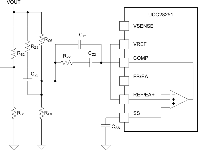 Figure 39. Error Amplifier Set Up For Secondary-Side Control
The error amplifier uses the lower voltage between the SS pin and the REF/EA+ pin to be the reference voltage for the feedback loop. In this method, the control loop is said to be ‘closed’ during the entire start up process, as it is always based on the true output voltage.
During soft start, the primary-side switch duty cycle is controlled by the COMP pin voltage and ramp voltage generated on the RAMP/CS pin. A higher COMP pin voltage results in larger duty cycle. However, to improve start up performance, the secondary-side synchronous rectifier duty cycle is controlled by a separate, internal ramp signal (generated by a dedicated pre-biased start up loop) and by the COMP pin voltage. This dedicated pre-biased loop is much faster than the regular voltage loop in order to avoid interaction between the two loops. The start up loop reads the output voltage via a transconductance error amplifier connected to the VSENSE pin. When the output voltage is higher than the reference, the pre-biased start up loop increases the SR duty cycle to reduce the output voltage. Conversely, when the output voltage is lower than the reference, the SR duty cycle is decreased to help maintain higher output voltage. To speed up the start up time, the minimum duty cycle of the synchronous rectifier is 50%.
Once the soft start is finished, the pre-biased loop is disabled and the duty cycle of the synchronous rectifiers becomes the complimentary of primary switches’ duty cycle, with some dead time inserted in between.
9.1.2.2 Primary-Side Control
When the UCC28251 is sitting on the primary side, the internal error amplifier is connected as a voltage follower and an extra error amplifier is needed on the secondary side for closed loop control. The error amplifier implementation is shown in Figure 40.
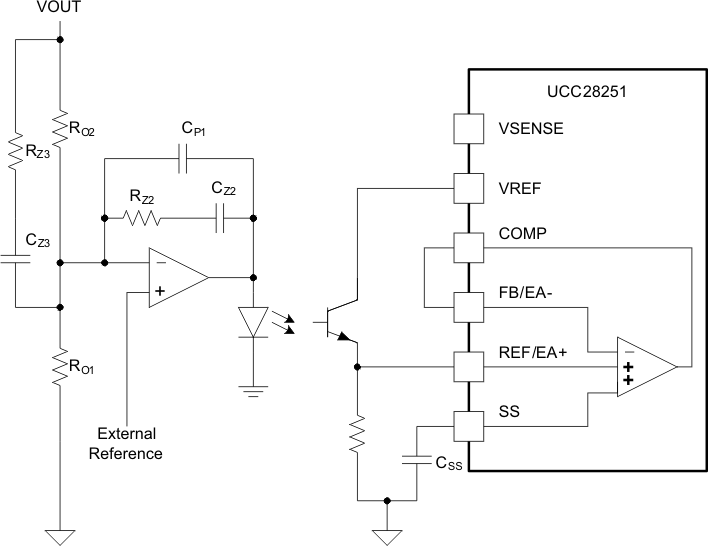 Figure 40. Error Amplifier Setup for Primary-Side Control
In the above configuration, the UCC28251 can only see the control loop feedback voltage, and cannot directly access the output voltage. The design of the soft-start time is critical to achieve optimal pre-biased start up performance. Some trial and error approaches are needed to achieve optimal performance. It is also important to choose the appropriate ramp amplitude. Refer to the ramp section discussion on the detailed design procedure for choosing ramp generation components.
During soft start, regardless of the pre-biased condition, the output voltage is always lower than the regulation voltage, so that the feedback loop is always saturated. When the internal error amplifier is connected as a voltage follower, the COMP voltage follows the lower of the voltage on the RER/EA+ pin and the SS pin. Since the feedback loop is saturated, the COMP pin always follows the SS pin voltage, until the output voltage becomes regulated and the feedback voltage takes over. In this control method, the output voltage control loop is always saturated, and the controller soft starts the COMP pin voltage. Therefore, it is called open loop soft start.
The primary-side switch duty cycle is controlled by the COMP pin voltage and by the RAMP/CS pin voltage. During soft start, the COMP pin voltage follows the SS pin as it is rising, so the primary-side switch duty cycle keeps increasing. When the output voltage becomes regulated, the feedback voltage becomes less than the SS pin voltage and the primary-side switch comes controlled by the control loop.
For the primary-side control setup, because output voltage is not directly accessible, the internal pre-biased start up loop is disabled by connecting VSENSE to VREF. Instead, the internal ramp used to generate the synchronous rectifier duty cycle is fixed, with the peak voltage of 3 V. The duty cycle of the synchronous rectifier increases as the SS pin voltage increases. When the SS pin voltage reaches 2.9 V, the soft start is considered finished and the synchronous rectifier duty cycle becomes the complementary of the primary-side switch duty cycle, minus the programmed dead time. Because of different COMP pin voltages at different line voltages, the SR duty cycle generated by the internal ramp might be different than the complementary of the primary-side switch duty cycle (1-D). If the duty cycle is too large, the internal logic is able to limit the duty cycle to (1-D). However, if the duty cycle is too small, when the soft start is finished, the SR duty cycle has a sudden change, which will cause output voltage disturbance. To optimize the pre-biased start up performance, it is recommended that the duty cycle change at the end of soft start be as small as possible.
9.1.3 Voltage Mode Control and Input Voltage Feed-Forward
For voltage mode control, a resistor RCS and a capacitor CCS are connected externally at RAMP/CS pin as shown in Figure 41. A ramp signal is generated on the RAMP/CS pin, at a rate of two times that of the switching frequency. The generated ramp signal is used to control the duty cycle for both the primary-side switches and secondary-side synchronous rectifiers. The ramp amplitude can be fixed or variable with the input voltage (input voltage feedforward).
To realize a fixed amplitude ramp, connect RCS to the constant voltage source, so that the ramp capacitor charging voltage is fixed regardless of line and load condition. The RAMP/CS pin is clamped internally to 4 V for internal device protection. Because the internal pull-down switch has about 40-Ω on-resistance, the CCS value must be small enough to discharge RAMP/CS from the peak to ground within TD(sp) + 70 ns (i.e. the pulse width of BLANK signal).
To achieve the input voltage feedforward, the slope of the ramp needs to be proportional to the input voltage. Tie RCS to the input line voltage. Because the ramp voltage is much lower than the input voltage, the ramp capacitor charging current is considered to be proportional to the input voltage. With input voltage feedforward, the COMP pin voltage should only move slightly even with large input voltage variation. This will provide much better line transient response for the converter.
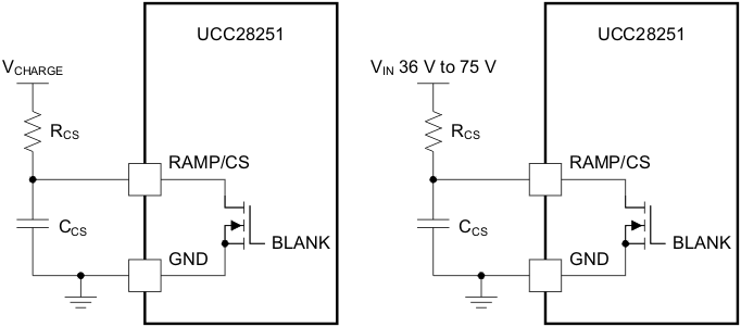 Figure 41. External Configuration Of RAMP/CS Pin With/Without Feed-Forward Operation
The input voltage feedforward also helps on pre-biased start up. When doing primary-side control to pre-biased start up, three conditions need to be considered:
9.1.3.1 Condition 1
At initial start up the primary side needs to provide enough energy to prevent output voltage dip;
9.1.3.2 Condition 2
At the end of soft start, it is required to keep the SR duty cycle change to be as small as possible. With input voltage feedforward, the COMP pin voltage is virtually fixed for different input voltages. Therefore, before the end of soft start, the duty cycle is the same for different input voltages. Choose the RCS and CCS following the procedure below.
Considering initial start up, the RAMP peak voltage should be:

In this equation, VIN is the input voltage because of the feedforward any input voltage should be fine; VPRE-BIAS is the highest pre-bias start-up voltage required by the system; n is the tranformer primary to secondary turns ratio and VSR(ramp) is the internal SR ramp peak voltage 3 V.
Another consideration is at the end of soft start, the SR duty cycle changes from controlled by the soft start, to complimentary to the primary-side duty cycle. The design should keep the transition as smooth as possible. Considering this, based on the output voltage and input voltage range, as well as the transformer turns ratio, calculate the SR duty cycle at different line voltages.
Next, based on the maximum duty cycle on the SR_DMAX, and the internal fixed ramp amplitude 3 V, the COMP voltage at regulation can be chosen as:

9.1.3.3 Condition 3
Use the calculated COMP pin voltage to derive the external ramp amplitude

According to the calculated ramp voltage from Equation 22 and Equation 24 some trade off is required to pick up the appropriate ramp voltage. Based on the selected ramp capacitor CCS value, choose the ramp resistor RCS value:

In this equation, VIN(max) is the maximum input voltage, fSW is the switching frequency.
Because these calculations ignore the dead time and the non-linearity of the ramp, slight modification is expected to achieve the optimal design. When the input voltage feed forward is not used, refer to the RAMP pin discussion for RC calculation.
9.1.4 Peak Current Mode Control
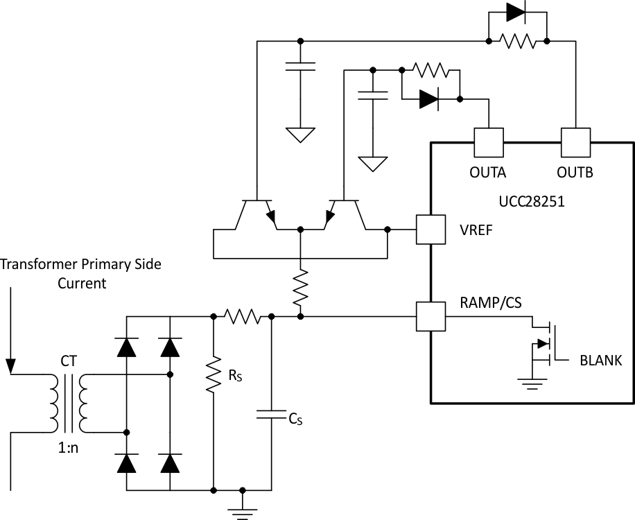
For peak current mode control, RAMP/CS pin is connected directly with the current signal generated from a current transformer. The current signal must be compatible with the input range of the COMP pin. External slope compensation is required to prevent sub-harmonic oscillation and to maintain flux-balance. The slope compensation can be implemented by using OUTA and OUTB to charge external capacitors and use the voltage follower to add into the sensed the current signal, as shown in Figure 42. Follow the peak current mode control theory to select compensation slope or refer to Modeling, Analysis and Compensation of the Current-Mode Converter (SLUA101).
9.1.5 Cycle-by-Cycle Current Limit and Hiccup Mode Protection
Cycle-by-cycle current limit is accomplished using the ILIM pin for both current mode control and voltage mode control. The input to the ILIM pin represents the primary current information. If the voltage sensed at ILIM pin exceeds 0.5 V, the current sense comparator terminates the pulse of output OUTA or OUTB. If the high current condition persists, the controller operates in a cycle-by-cycle current limit mode with duty cycle determined by the current sense comparator instead of the PWM comparator. ILIM pin is pulled down by an internal switch at the rising edge of each clock cycle. This internal switch remains on for an additional 70 ns after OUTA or OUTB goes high to blank leading edge transient noise in the current sensing loop. This reduces the filtering requirements at the ILIM pin and improves the current sense response time.
UCC28251 makes it possible to maintain flux balance during cycle-by-cycle current limit operation. The duty cycles of primary switches are always matched. If one switch duty cycle is terminated earlier because of current limiting, a matched duty cycle is applied to the other switch for the next half switching cycle, regardless of the current condition, as shown in Figure 43. This matched duty cycle helps to maintain volt-second balancing on the transformer and prevents the transformer saturation.
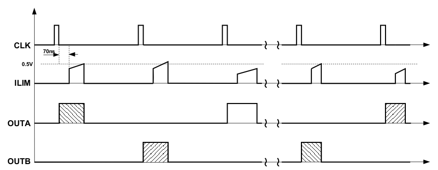 Figure 43. Cycle-by-Cycle Current Limit Duty Cycle Matching
Once the current limit is triggered, the 75-µA internal current source begins to charge the capacitor on HICC pin. If the current limit condition went away before HICC pin reaches 0.6 V, the device stops charge HICC capacitor and begins to discharge it with 2.7-µA current source. If the cycle-by-cycle current limit condition continues, HICC pin reachs 0.6 V, and all four outputs are shut down. The UCC28251 then enters hiccup mode. During hiccup mode, all four outputs keep low; SS pin is pulled to ground internally; a 2.7-µA current source continuously discharge HICC pin capacitor; until HICC pin voltage reaches 0.3 V. After that, HICC pin is discharged internally to get ready for the next HICC event. The whole converter starts with soft start after hiccup mode.
The cycle-by-cycle current limit operation time before all four outputs shut down is programmed by external capacitor CHICC at HICC pin. The delay time can be calculated as:

The hiccup timer keeps all outputs being zero until the timer expires. The hiccup time THICC is calculated as:

As soon as the outputs are shut-down, SS pin is pulled down internally until the hiccup restart timer is reset after time duration THICC. The detailed illustration of HICCUP mode is shown in Figure 44.
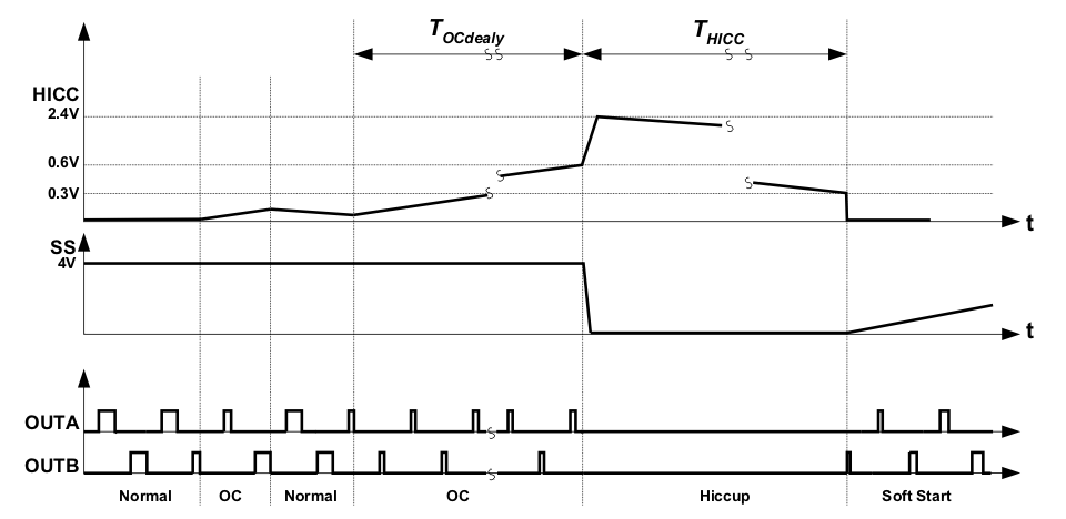 Figure 44. Cycle-By-Cycle Current Limit Delay Timer and Hiccup Restart Timer
9.2 Typical Applications
9.2.1 Circuit Diagram in Design Example
The example provided here is to show how to design a symmetrical half bridge converter of voltage mode control with UCC28251 on primary side.
Figure 45 is the circuit diagram to be used in this design example. This design example is to show how to determine the values in the circuit associated to UCC28251 programming.
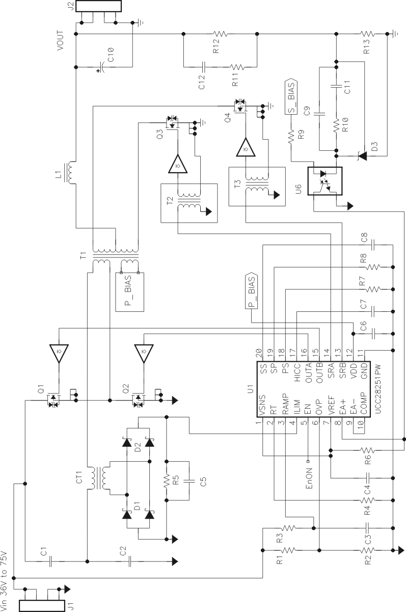 Figure 45. Circuit Diagram in Design Example
9.2.1.1 Design Requirements
Table 2 shows the specifications for the design example.
Table 2. Specifications for the Design Example
| PARAMETER | MIN | TYP | MAX | UNIT | |
|---|---|---|---|---|---|
| VIN | Input voltage | 36 | 48 | 72 | VDC |
| VOUT | Output voltage | 3.3 | |||
| POUT | Outpu power | 75 | W | ||
| IOUT | Output load current | 23 | A | ||
| COUT | Load capacitance | 5000 | µF | ||
| fSW | Switching frequency | 150 | kHz | ||
| PLIMIT | Over-power limit | 150% | |||
| η | Efficiancy at full load | 90% | |||
| Isolation | 1500 | V | |||
9.2.1.2 Detailed Design Procedure
9.2.1.2.1 Step 1: Power Stage Design
The power stage design in this example is standard and the same as that for symmetrical half bridge converter of voltage mode control. From the standard design, these components are determined. This includes Q1 through Q4, C1, C2, CT1, D1 and D2, D3, T1, T2 and T3, and U6. Their design is standard. Also, design associated to current sensing and protection is also standard. This includes CT1, D1, D2, R5 and C5.
9.2.1.2.2 Step 2: Feedback Loop Design
D3 (TLV431) with U6, R6, R9, R10, R12, R13, C11 and C12 are composed of standard type 3 feedback loop compensation network and output voltage set point. Their design is also standard.
9.2.1.2.3 Step 3: Programming The Device
9.2.1.2.3.1 Step 3-1
Equation 3 is used to determine RT based on switching frequency, 300 kHz and assumes the dead time of 150 ns.
9.2.1.2.3.2 Step 3-2: Determine Ramp Resistance and Capacitance
There are two-fold considerations to determine RAMP resistance and capacitance. Equation 22 provides RAMP consideration for SR initial start up with prebias. The corresponding RAMP peak voltage is determined with input voltage low line and maximum prebias output voltage. In the below T1 turns ratio n = 4.

Equation 23 and Equation 24 provides RAMP consideration for soft start completion to make duty cycle match (1-D) = SR_D.
- Calculate OUTA or OUTB duty cycle at 75-V input voltage, 3.3-V output.
- Calculate SRA or SRB duty cycle.
- Calculate the COMP voltage value in steady state (Equation 23).
- Calculate the RAMP peak value (Equation 24).
- Arbitrary select CRAMP 470 pF, then C3 = 470 pF.
- Calculate RRAMP.


As different RAMP resistor values are obtained, at this stage, we may take their average value for initial design.
9.2.1.2.4 Step 3-3: Determine Soft-Start Capacitance
Determine soft-start capacitance with soft-start time 15 ms.

9.2.1.2.5 Step 3-4: Determine Dead-Time Resistance
Assuming the dead time is 150 ns, Select R7 = R8 = 121 kΩ based on Figure 27 and Figure 28.
9.2.1.2.6 Step 3-5: Determine OCP Hiccup Off-Time Capacitance
Assuming off time is 0.8 s (Equation 14).

9.2.1.2.7 Step 3-6: Determine Primary-Side OVP Resistance
Assuming OV_OFF = 73 V, OV_ON = 72 V (Equation 15 to Equation 17).


9.2.1.2.8 Step 3-7: Select Capacitance for VDD and VREF
As recommended by the datasheet, select C6 = C4 = 1.0 µF. The final design is shown in Figure 46.
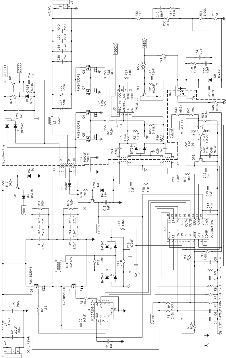 Figure 46. Schematics of Primary-Side Control Design Example
9.2.1.3 Application Curves
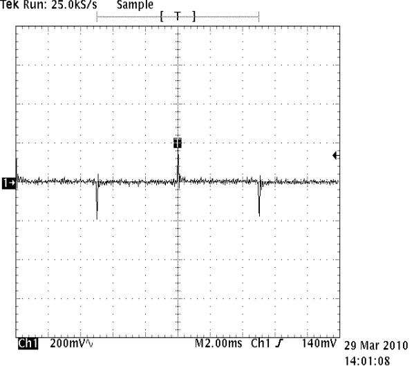 Figure 47. Load Transient
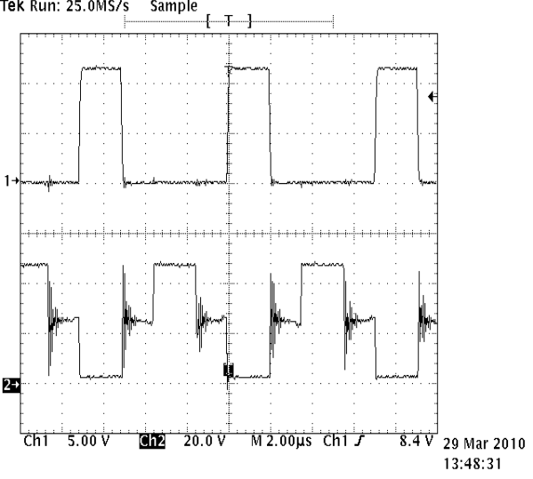 Figure 49. Clock Signal and Switching Node Waveform
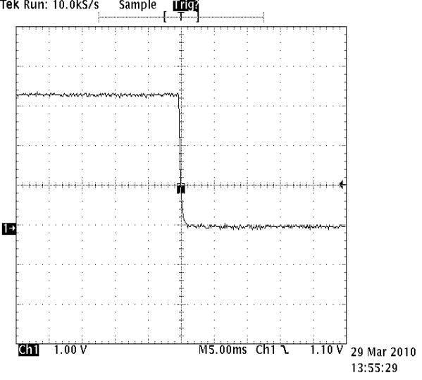 Figure 51. Enable Turn-Off Waveform
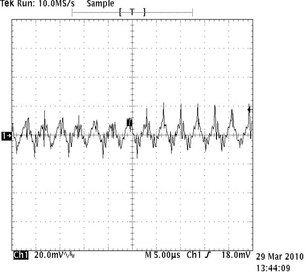 Figure 48. Output Ripple
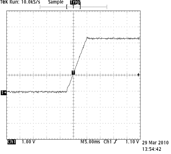 Figure 50. Enable Turn-On Waveform
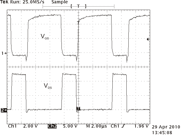 Figure 52. Secondary-Side Switching Waveform
9.2.2 Secondary-Side Half-Bridge Controller With Synchronous Rectification
UCC28250 also supports secondary-side control. Refer to Figure 53. In this configuration, the UCC28250 can be used in a design that produces smooth turn-on performance with an output pre-bias condition. The design example and guidelines are summarized in Designing UCC28250 as a Secondary Side Control for Output Turn-On with a Pre-Bias Condition, SLAA477, and Using the UCC28250EVM-564, SLUU441.
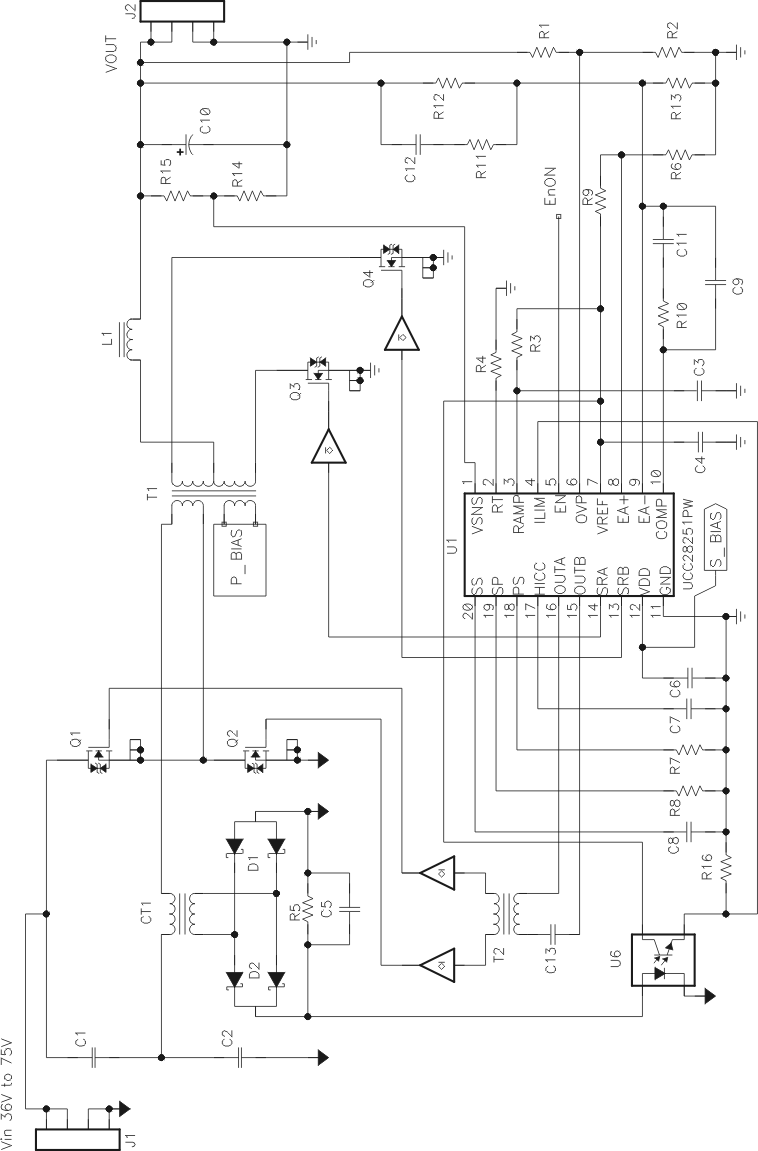 Figure 53. Secondary-Side Half-Bridge Controller With Synchronous Rectification
