SLUSBD8E February 2013 – December 2014 UCC28251
PRODUCTION DATA.
- 1 Features
- 2 Applications
- 3 Description
- 4 Revision History
- 5 Description (continued)
- 6 Pin Configuration and Functions
- 7 Specifications
-
8 Detailed Description
- 8.1 Overview
- 8.2 Functional Block Diagram
- 8.3
Feature Description
- 8.3.1 VDD (5/12)
- 8.3.2 VREF (Reference Generator) (20/7)
- 8.3.3 EN (Enable Pin) (18/5)
- 8.3.4 RT (Oscillator Frequency Set and Synchronization) (15/2)
- 8.3.5 SP (Synchronous Rectifier Turn-Off to Primary Output Turn-On Dead Time Programming) (13/19)
- 8.3.6 PS (Primary Output Turn-Off to Synchronous Rectifier Turn-On Dead Time Programming) (11/18)
- 8.3.7 RAMP/CS (PWM Ramp Input or Current Sense Input) (16/3)
- 8.3.8 REF/EA+ (1/8)
- 8.3.9 FB/EA- (2/9)
- 8.3.10 COMP (3/10)
- 8.3.11 VSENSE (14/1)
- 8.3.12 SS (Soft Start Programming Pin) (13/20)
- 8.3.13 ILIM (Current Limit for Cycle-by-Cycle Over-Current Protection) (17/4)
- 8.3.14 HICC (10/17)
- 8.3.15 OVP/OTP (19/6)
- 8.3.16 OUTA (9/16) and OUTB (8/15)
- 8.3.17 SRA (7/14) and SRB (6/13)
- 8.3.18 GND (4/11)
- 8.4 Device Functional Modes
-
9 Application and Implementation
- 9.1 Application Information
- 9.2
Typical Applications
- 9.2.1
Circuit Diagram in Design Example
- 9.2.1.1 Design Requirements
- 9.2.1.2
Detailed Design Procedure
- 9.2.1.2.1 Step 1: Power Stage Design
- 9.2.1.2.2 Step 2: Feedback Loop Design
- 9.2.1.2.3 Step 3: Programming The Device
- 9.2.1.2.4 Step 3-3: Determine Soft-Start Capacitance
- 9.2.1.2.5 Step 3-4: Determine Dead-Time Resistance
- 9.2.1.2.6 Step 3-5: Determine OCP Hiccup Off-Time Capacitance
- 9.2.1.2.7 Step 3-6: Determine Primary-Side OVP Resistance
- 9.2.1.2.8 Step 3-7: Select Capacitance for VDD and VREF
- 9.2.1.3 Application Curves
- 9.2.2 Secondary-Side Half-Bridge Controller With Synchronous Rectification
- 9.2.1
Circuit Diagram in Design Example
- 10Power Supply Recommendations
- 11Layout
- 12Device and Documentation Support
- 13Mechanical, Packaging, and Orderable Information
Package Options
Mechanical Data (Package|Pins)
Thermal pad, mechanical data (Package|Pins)
- RGP|20
Orderable Information
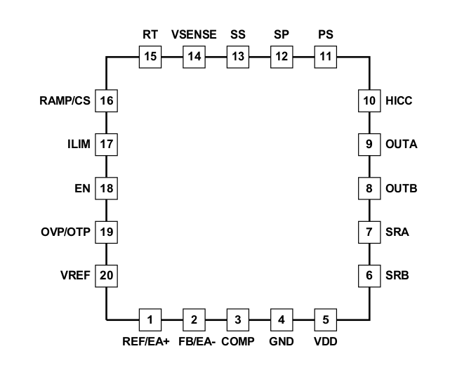
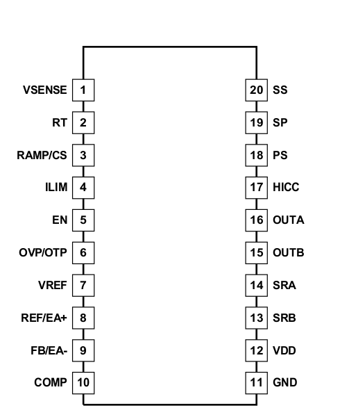
6 Pin Configuration and Functions


Pin Functions
| PIN | I/O | DESCRIPTION | ||
|---|---|---|---|---|
| QFN-20 | PW-20 | NAME | ||
| 5 | 12 | VDD | I | Bias supply input. |
| 20 | 7 | VREF | O | 3.3-V reference output. |
| 18 | 5 | EN | I | Device enable and disable. |
| 15 | 2 | RT | I | Oscillator frequency set or synchronous clock input. |
| 12 | 19 | SP | I | Synchronous rectifier off to primary on dead-time set . |
| 11 | 18 | PS | I | Primary off to synchronous rectifier on dead-time set . |
| 16 | 3 | RAMP/CS | I | PWM ramp input (for voltage mode control) or current sense input (for current mode control). |
| 1 | 8 | REF/EA+ | I | Error amplifier non-inverting input. |
| 2 | 9 | FB/EA- | I | Error amplifier inverting input. |
| 3 | 10 | COMP | I/O | Error amplifier output. |
| 14 | 1 | VSENSE | I | Output voltage sensing for pre-bias control. |
| 13 | 20 | SS | I/O | Soft-start programming. |
| 17 | 4 | ILIM | I | Current sense for cycle-by-cycle over-current protection. |
| 10 | 17 | HICC | I | Cycle-by-cycle current limit time delay and Hiccup time setting. |
| 19 | 6 | OVP/OTP | I | Over voltage and over temperature protection pin. |
| 9 | 16 | OUTA | O | 0.2-A sink/source primary switching output. |
| 8 | 15 | OUTB | O | 0.2-A sink/source primary switching output. |
| 7 | 14 | SRA | O | 0.2-A sink/source synchronous rectifier output. |
| 6 | 13 | SRB | O | 0.2-A sink/source synchronous rectifier output. |
| 4 | 11 | GND | I | Ground. |