SLUS888G JANUARY 2009 – September 2015 UCC28610
PRODUCTION DATA.
- 1 Features
- 2 Applications
- 3 Description
- 4 Revision History
- 5 Pin Configuration and Functions
- 6 Specifications
- 7 Detailed Description
- 8 Application and Implementation
- 9 Power Supply Recommendations
- 10Layout
- 11Device and Documentation Support
- 12Mechanical, Packaging, and Orderable Information
Package Options
Mechanical Data (Package|Pins)
- D|8
Thermal pad, mechanical data (Package|Pins)
Orderable Information
6 Specifications
6.1 Absolute Maximum Ratings
All voltages are with respect to GND, –40°C < TJ = TA < 125°C, all currents are positive into and negative out of the specified terminal (unless otherwise noted) (1)| MIN | MAX | UNIT | |||
|---|---|---|---|---|---|
| Input voltage range | VDD | –0.5 | 25 | V | |
| DRV, during conduction | –0.5 | 2.0 | |||
| DRV, during non-conduction | 20 | ||||
| VGG (2) | –0.5 | 16 | |||
| ZCD, MOT, CL (3) | –0.5 | 7 | |||
| FB (3) | –0.5 | 1.0 | |||
| VDD – VGG | –7 | 10 | |||
| Continuous input current | IVGG (2) | 10 | mA | ||
| Input current range | IZCD, IMOT, ICL, IFB (3) | –3 | 1 | ||
| Peak output current | DRV | -5 | A | ||
| DRV, pulsed 200ns, 2% duty cycle | –5 | 1.5 | |||
| TJ | Operating junction temperature, | –40 | 150 | °C | |
| Lead Temperature (soldering, 10 sec.) | 260 | °C | |||
| Tstg | Storage temperature range | –65 | 150 | °C | |
(1) These are stress ratings only. Stress beyond these limits may cause permanent damage to the device. Functional operation of the device at these or any conditions beyond those indicated under Recommended Operating Conditions is not implied. Exposure to absolute maximum rated conditions for extended periods of time may affect device reliability
(2) Voltage on VGG is internally clamped. The clamp level varies with operating conditions. In normal use, VGG is current fed with the voltage internally limited
6.2 ESD Ratings
| VALUE | UNIT | |||
|---|---|---|---|---|
| V(ESD) | Electrostatic discharge | Human body model (HBM), per ANSI/ESDA/JEDEC JS-001, all pins (1) | 1500 | V |
| Charged device model (CDM), per JEDEC specification JESD22-C101, all pins (2) | 500 | |||
(1) JEDEC document JEP155 states that 500-V HBM allows safe manufacturing with a standard ESD control process.
(2) JEDEC document JEP157 states that 250-V CDM allows safe manufacturing with a standard ESD control process.
6.3 Recommended Operating Conditions
Unless otherwise noted, all voltages are with respect to GND, -40°C < TJ = TA < 125°C. Components reference, Figure 34.| MIN | MAX | UNIT | |||
|---|---|---|---|---|---|
| VDD | Input voltage | 9 | 20 | V | |
| VGG | Input voltage from low-impedance source | 9 | 13 | V | |
| IVGG | Input current from a high-impedance source | 10 | 2000 | μA | |
| RMOT | Resistor to GND | Shutdown/Retry mode | 25 | 100 | kΩ |
| Latch-off mode | 150 | 750 | kΩ | ||
| RCL | Resistor to GND | 24.3 | 100 | kΩ | |
| RZCD1 | Resistor to auxiliary winding | 50 | 200 | kΩ | |
| CVGG | VGG capacitor | 33 | 200 | nF | |
| CBP | VDD bypass capacitor, ceramic | 0.1 | 1 | μF | |
6.4 Thermal Information
| THERMAL METRIC (1) | UCC28610 | UNIT | ||
|---|---|---|---|---|
| D (SOIC) | P (PDIP) | |||
| 8 PINS | 8 PINS | |||
| RθJA | Junction-to-ambient thermal resistance | 117.5 | 56.3 | °C/W |
| RθJC(top) | Junction-to-case (top) thermal resistance | 63.7 | 45.7 | °C/W |
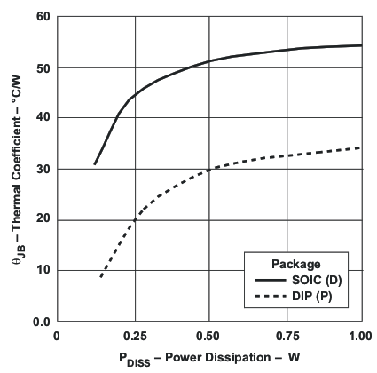
| RθJB | Junction-to-board thermal resistance | 57.8 | 33.5 | °C/W |
| ψJT | Junction-to-top characterization parameter | 15.3 | 22.9 | °C/W |
| ψJB | Junction-to-board characterization parameter | 57.3 | 33.4 | °C/W |
(1) For more information about traditional and new thermal metrics, see the Semiconductor and IC Package Thermal Metrics application report, SPRA953.
6.5 Electrical Characteristics
Unless otherwise stated: VDD = 12 V, VGG = 12 V, ZCD = 1 V, IFB = 10 µA, GND = 0 V, a 0.1-μF capacitor between VDD and GND, a 0.1-μF capacitor between VGG and GND, RCL = 33.2 kΩ, RMOT = 380 kΩ, –40°C < TA < +125°C, TJ = TA| PARAMETER | TEST CONDITIONS | MIN | TYP | MAX | UNIT | |
|---|---|---|---|---|---|---|
| VDD and VGG SUPPLY | ||||||
| VGG(OPERATING) | VGG voltage, operating | VDD = 14 V, IVGG = 2.0 mA | 13 | 14 | 15 | V |
| VGG(DISABLED) | VGG voltage, PWM disabled | VDD = 12 V, IVGG = 15 μA, IFB = 350 μA | 15 | 16 | 17 | V |
| ΔVGG | Rise in VGG clamping voltage during UVLO, GM, or Fault | VGG(DISABLED) – VGG(OPERATING) | 1.75 | 2.00 | 2.15 | V |
| IVGG(SREG) | VGG shunt regulator current | VGG = VGG(DISABLED) -100 mV, VDD = 12 V | 6 | 10 | μA | |
| ΔVGG(SREG) | VGG shunt load regulation | 10 μA ≤ IVGG ≤ 5 mA, IFB = 350 μA | 125 | 200 | mV | |
| VGG(LREG) | VGG LDO regulation voltage | VDD = 20 V, IVGG = – 2 mA | 13 | V | ||
| VGG(LREG, DO) | VGG LDO Dropout Voltage | VDD – VGG, VDD = 11 V, IVGG = – 2 mA | 1.5 | 2 | 2.5 | V |
| VDD(ON) | UVLO turn-on threshold | 9.7 | 10.2 | 10.7 | V | |
| VDD(OFF) | UVLO turn-off threshold | 7.55 | 8 | 8.5 | V | |
| ΔVDD(UVLO) | UVLO hysteresis | 1.9 | 2.2 | 2.5 | V | |
| IVDD(OPERATING) | Operating current | VDD = 20 V | 2.5 | 3 | 3.7 | mA |
| IVDD(GM) | Idle current between bursts | IFB = 350 μA | 550 | 900 | μA | |
| IVDD(UVLO) | Current for VDD < UVLO | VDD = VDD(ON) – 100 mV, increasing | 225 | 310 | μA | |
| RDS,ON(VDD) | VDD Switch on resistance, DRV to VDD | VGG = 12 V, VDD = 7V, IDRV = 50 mA | 4 | 10 | Ω | |
| VDD(FAULT RESET) | VDD for fault latch reset | 5.6 | 6 | 6.4 | V | |
| MODULATION | ||||||
| tS(HF) (1) | Minimum switching period, frequency modulation (FM) mode | IFB = 0 μA, (1) | 7.125 | 7.5 | 7.875 | μs |
| tS(LF) (1) | Maximum switching period, reached at end of FM modulation range | IFB = IFB, CNR3 – 20 μA, (1) | 31 | 34 | 38 | μs |
| IDRVpk(max) | Maximum peak driver current over amplitude modulation(AM) range | IFB = 0 μA, RCL = 33. 2 kΩ | 2.85 | 3 | 3.15 | A |
| IFB = 0 μA, RCL = 100 kΩ | 0.80 | 0.90 | 1.0 | |||
| IDRVpk(min) | Minimum peak driver current reached at end of AM modulation range | IFB, CNR2 + 10 μA, RCL = 33.2 kΩ | 0.7 | 0.85 | 1.1 | A |
| IFB, CNR2 + 10 μA, RCL = 100 kΩ | 0.2 | 0.33 | 0.5 | |||
| KP | Maximum power constant | IDRVpk(max) = 3 A | 0.54 | 0.60 | 0.66 | W/μH |
| IDRVpk(absmin) | Minimum peak driver independent of RCL or AM control | RCL = OPEN | 0.3 | 0.45 | 0.6 | A |
| tBLANK(Ilim) | Leading edge current limit blanking time | IFB = 0 μA, RCL = 100 kΩ, 1.2-A pull-up on DRV | 120 | 220 | 450 | ns |
| VCL | Voltage of CL pin | IFB = 0 μA | 2.94 | 3 | 3.06 | V |
| IFB = (IFB,CNR3 – 20 μA) (1) | 0.95 | 1.00 | 1.10 | |||
| IFB,CNR1 (4) | IFB range for FM modulation | IFB increasing, tS = tS(LF), IDRVpk = IDRVpk(max) |
145 | 165 | 195 | μA |
| IFB,CNR2 – IFB,CNR1 (4) | IFB range for AM modulation | tS = tS(LF), IDRVpk ranges from IDRVpk(max) to IDRVpk(min) |
35 | 45 | 65 | μA |
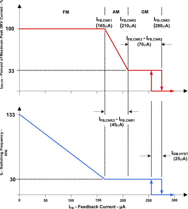
| IFB,CNR3 – IFB,CNR2 (4) | IFB range for Green Mode (GM) modulation | IFB increasing until PWM action is disabled entering a burst-off state | 45 | 70 | 90 | μA |
| IFB, GM-HYST (4) | IFB hysteresis during GM modulation to enter burst on and off states | IFB decreasing from above IFB,CNR3 | 10 | 25 | 40 | μA |
| VFB | Voltage of FB pin | IFB = 10 μA | 0.34 | 0.7 | 0.84 | V |
| ZERO CROSSING DETECTION | ||||||
| ZCD(TH) | ZCD zero crossing threshold | ZCD high to low generates switching period (tS has expired) | 5 | 20 | 50 | mV |
| ZCD(CLAMP) | ZCD low clamp voltage | IZCD = –10 μA | -220 | -160 | -100 | mV |
| ZCD(START) | ZCD voltage threshold to enable the internal start timer | Driver switching periods generated at start timer rate | 0.1 | 0.15 | 0.2 | V |
| tDLY(ZCD) | Delay from zero crossing to Driver turn-on | 150-Ω pull-up to 12-V on DRV | 150 | ns | ||
| tWAIT(ZCD) | Wait time for zero crossing detection | Driver turn-on edge generated following tS with previous zero crossing detected | 2 | 2.4 | 2.8 | μs |
| tST | Starter time-out period | ZCD = 0 V | 150 | 240 | 300 | |
| DRIVER | ||||||
| RDS(on)(DRV) | Driver on-resistance | IDRV = 4.0 A | 90 | 190 | mΩ | |
| IDRV(OFF) | Driver off-leakage current | DRV = 12 V | 1.5 | 20 | μA | |
| RDS(on)(HSDRV) | High-side driver on-resistance | IDRV = –50 mA | 6 | 11 | Ω | |
| IDRV(DSCH) | DRV bulk discharge current | VDD open, DRV= 12 V, Fault latch set | 2 | 2.8 | 3.6 | mA |
| OVERVOLTAGE FAULT | ||||||
| ZCD(OVP) | Overvoltage fault threshold at ZCD | Fault latch set | 4.85 | 5 | 5.15 | V |
| tBLANK(OVP) | ZCD blanking and OVP sample time from the turn-off edge of DRV | 0.6 | 1 | 1.7 | μs | |
| IZCD(bias) | ZCD Input bias current | ZCD = 5 V | -0.1 | -0.05 | 0.1 | μA |
| OVERLOAD FAULT | ||||||
| IFB(OL) | Current to trigger overload delay timer | 0 | 1.5 | 3 | μA | |
| tOL | Delay to overload fault | IFB = 0 A continuously | 200 | 250 | 325 | ms |
| tRETRY | Retry delay in retry mode or after shutdown command | RMOT = 76 kΩ | 750 | ms | ||
| RMOT(TH) | Boundary RMOT between latch-off and retry modes | See (2) | 100 | 120 | 150 | kΩ |
| SHUTDOWN THRESHOLD | ||||||
| MOT(SR) | Shutdown-Retry threshold | MOT high to low | 0.7 | 1 | 1.3 | V |
| IMOT | MOT current when MOT is pulled low | MOT = 1 V | –600 | –450 | –300 | μA |
| MAXIMUM ON TIME | ||||||
| tMOT | Latch-OFF | RMOT = 383 kΩ | 3.43 | 3.83 | 4.23 | μs |
| Shutdown-retry | RMOT = 76 kΩ | 3.4 | 3.8 | 4.2 | ||
| MOT | MOT voltage | 2.7 | 3 | 3.3 | V | |
| THERMAL SHUTDOWN | ||||||
| TSD (3) | Shutdown temperature | TJ, temperature rising (3) | 165 | °C | ||
| TSD_HYS (3) | Hysteresis | TJ, temperature falling, degrees below TSD (3) | 15 | °C | ||
(1) tS sets a minimum switching period. Following the starting edge of a PWM on time, under normal conditions, the next on time is initiated following the first zero crossing at ZCD after tS. The value of tS is modulated by IFB between a minimum of tS(HF) and a maximum of tS(LF) In normal operation, tS(HF) sets the maximum operating frequency of the power supply and tS(LF) sets the minimum operating frequency of the power supply.
(2) A latch-off or a shutdown and retry fault response to a sustained overload is selected by the range of RMOT.
To select the latch-off mode, RMOT should be greater than 150 kΩ and tMOT is given by RMOT × (1.0 × 10⁻¹¹).
To select the shutdown-retry mode, RMOT should be less than 100 kΩ and tMOT is given by RMOT × (5.0 × 10⁻¹¹).
To select the latch-off mode, RMOT should be greater than 150 kΩ and tMOT is given by RMOT × (1.0 × 10⁻¹¹).
To select the shutdown-retry mode, RMOT should be less than 100 kΩ and tMOT is given by RMOT × (5.0 × 10⁻¹¹).
(3) Thermal shutdown occurs at temperatures higher than the normal operating range. Device performance at or near thermal shutdown temperature is not specified or assured.
(4) Refer to Figure 1.
6.6 Typical Characteristics
Unless otherwise stated: VDD = 12 V, VGG = 12 V, ZCD = 1 V, IFB = 10 µA, GND = 0 V, a 0.1-μF capacitor between VDD and GND, a 0.1-μF capacitor between VGG and GND, RCL = 33.2 kΩ, RMOT = 380 kΩ, –40°C < TA < +125°C, TJ = TA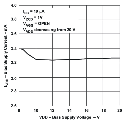 Figure 2. Bias Supply Current vs Bias Supply Voltage During Operation
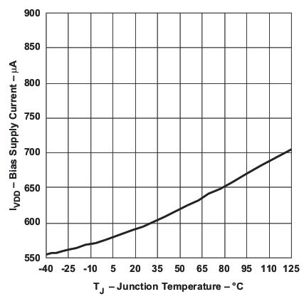 Figure 4. Bias Supply Current vs Temperature During Green Mode
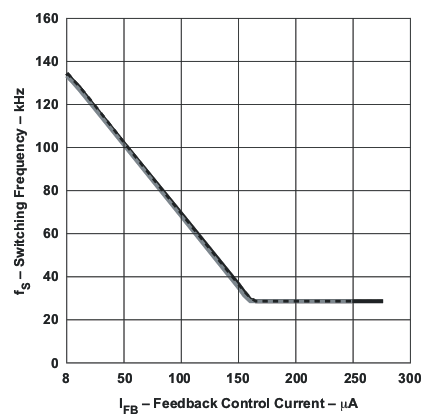 Figure 6. Oscillator Frequency vs Feedback Current
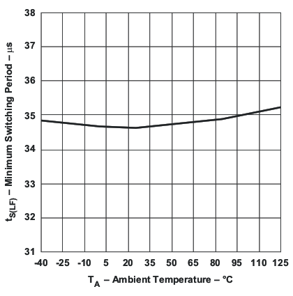 Figure 8. Switching Period During Amplitude Modulaltion vs Ambient Temperature
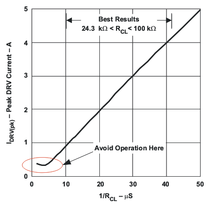 Figure 10. Peak DRV Current vs Transconductance (1/RCL)
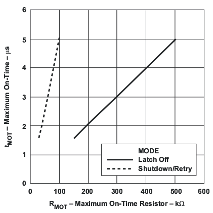 Figure 12. Maximum On Time vs Maximum On-Time Resistance
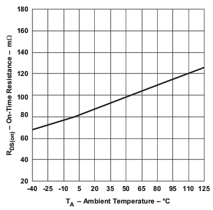 Figure 14. Driver RDS(on) vs Ambient Temperature
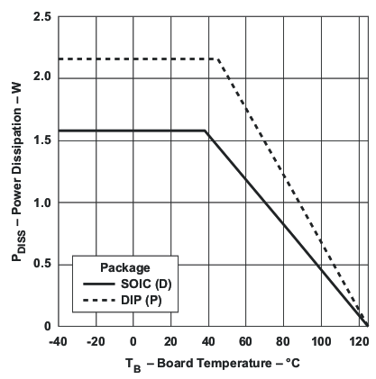 Figure 16. Safe Operating Area vs Board Temperature
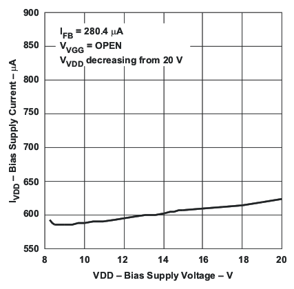 Figure 3. Bias Supply Current vs Bias Supply Voltage During Green Mode
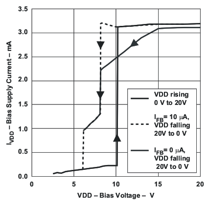 Figure 5. Operational IVDD – Bias Current vs Bias Voltage
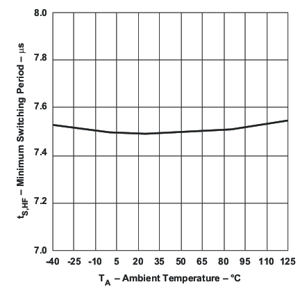 Figure 7. Minimum Switching Period vs Temperature
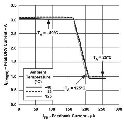 Figure 9. Peak DRV Current vs Feedback Current
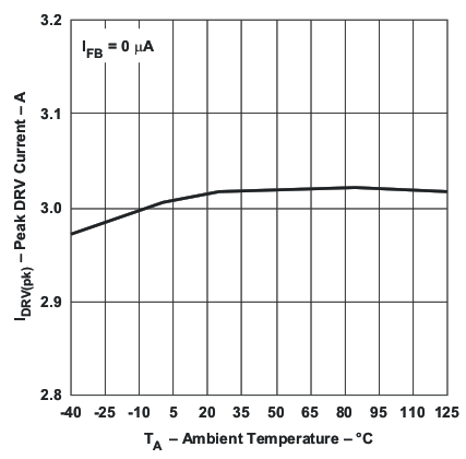 Figure 11. Peak DRV Current vs Ambient Temperature
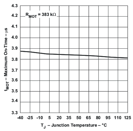 Figure 13. Maximum On Time vs Junction Temperature
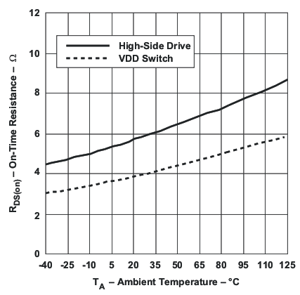 Figure 15. RDS(on) of High Side Drive and VDD Switch vs Temperature
