SLUSB41A July 2012 – December 2014 UCC28700 , UCC28701 , UCC28702 , UCC28703
PRODUCTION DATA.
- 1 Features
- 2 Applications
- 3 Description
- 4 Revision History
- 5 Device Comparison Table
- 6 Pin Configuration and Functions
- 7 Specifications
- 8 Detailed Description
-
9 Applications and Implementation
- 9.1 Application Information
- 9.2
Typical Application
- 9.2.1 Design Requirements
- 9.2.2
Detailed Design Procedure
- 9.2.2.1 Transformer Parameter Verification
- 9.2.2.2 Output Capacitance
- 9.2.2.3 VDD Capacitance, CDD
- 9.2.2.4 VDD Start-Up Resistance, RSTR
- 9.2.2.5 VS Resistor Divider, Line Compensation, and Cable Compensation
- 9.2.2.6 Input Bulk Capacitance and Minimum Bulk Voltage
- 9.2.2.7 Transformer Turns Ratio, Inductance, Primary-Peak Current
- 9.2.2.8 Standby Power Estimate
- 9.2.3 Application Curves
- 10Power Supply Recommendations
- 11Layout
-
12Device and Documentation Support
- 12.1
Device Support
- 12.1.1
Device Nomenclature
- 12.1.1.1 Capacitance Terms in Farads
- 12.1.1.2 Duty Cycle Terms
- 12.1.1.3 Frequency Terms in Hertz
- 12.1.1.4 Current Terms in Amperes
- 12.1.1.5 Current and Voltage Scaling Terms
- 12.1.1.6 Transformer Terms
- 12.1.1.7 Power Terms in Watts
- 12.1.1.8 Resistance Terms in Ω
- 12.1.1.9 Timing Terms in Seconds
- 12.1.1.10 Voltage Terms in Volts
- 12.1.1.11 AC Voltage Terms in VRMS
- 12.1.1.12 Efficiency Terms
- 12.1.1
Device Nomenclature
- 12.2 Documentation Support
- 12.3 Trademarks
- 12.4 Electrostatic Discharge Caution
- 12.5 Glossary
- 12.1
Device Support
- 13Mechanical, Packaging, and Orderable Information
Package Options
Mechanical Data (Package|Pins)
- DBV|6
Thermal pad, mechanical data (Package|Pins)
Orderable Information
11 Layout
11.1 Layout Guidelines
 Figure 28. 5W USB Adapter Schematic
- High frequency bypass Capacitor C7 should be placed arcos Pin 2 and 5 as close as you can get it to the pins.
- Resistor R15 and C7 form a low pass filter and the connection of R15 and C7 should be as close to the VDD pin as possible.
- C9 should be put as close to CS pin and R10 as possible. This forms a low pass filter with R10.
- The connection for C9 and R10 should be as close to the CS pin as possible.
- Please note that C9 may not be required in all designs. However, it is wise to put a place holder for it in your design.
- The VS pin controls the output voltage through the transformer turns ratio and the voltage divider of R7 and R9. Note the trace with between the R7, R9 and VS pin should be; as short as; possible to reduce/eliminate possible EMI coupling.
- Note the IC ground and power ground should meet at the bulk capacitor’s (C4 and C5) return. Tri to ensure that high frequency/high current from the power stage does not go through the signal ground.
- The high frequency/high current path that you need to be cautious of on the primary is C4, C5 +, T1 (P1,P2), Q1d, Q1s, R13 to the return of C4 and C5.
- Try to keep all high current loops as short as possible.
- Keep all high current/high frequency traces away from or perpendicular to other traces in the design.
- Traces on the voltage clamp formed by D1, R1, D4 and C4 as short as possible.
- C4 return needs to be as close to the bulk capacitor supply as possible. This reduces the magnitude of dv/dt caused by large di/dt.
- Avoid mounting semiconductors under magnetics.
11.2 Layout Example
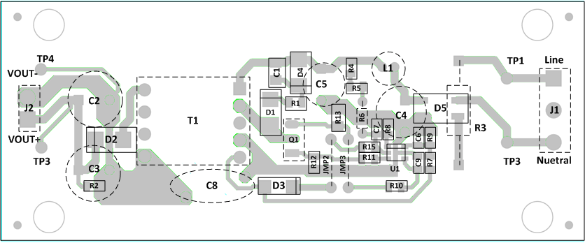 Figure 29. Layout Example