SLUSB41A July 2012 – December 2014 UCC28700 , UCC28701 , UCC28702 , UCC28703
PRODUCTION DATA.
- 1 Features
- 2 Applications
- 3 Description
- 4 Revision History
- 5 Device Comparison Table
- 6 Pin Configuration and Functions
- 7 Specifications
- 8 Detailed Description
-
9 Applications and Implementation
- 9.1 Application Information
- 9.2
Typical Application
- 9.2.1 Design Requirements
- 9.2.2
Detailed Design Procedure
- 9.2.2.1 Transformer Parameter Verification
- 9.2.2.2 Output Capacitance
- 9.2.2.3 VDD Capacitance, CDD
- 9.2.2.4 VDD Start-Up Resistance, RSTR
- 9.2.2.5 VS Resistor Divider, Line Compensation, and Cable Compensation
- 9.2.2.6 Input Bulk Capacitance and Minimum Bulk Voltage
- 9.2.2.7 Transformer Turns Ratio, Inductance, Primary-Peak Current
- 9.2.2.8 Standby Power Estimate
- 9.2.3 Application Curves
- 10Power Supply Recommendations
- 11Layout
-
12Device and Documentation Support
- 12.1
Device Support
- 12.1.1
Device Nomenclature
- 12.1.1.1 Capacitance Terms in Farads
- 12.1.1.2 Duty Cycle Terms
- 12.1.1.3 Frequency Terms in Hertz
- 12.1.1.4 Current Terms in Amperes
- 12.1.1.5 Current and Voltage Scaling Terms
- 12.1.1.6 Transformer Terms
- 12.1.1.7 Power Terms in Watts
- 12.1.1.8 Resistance Terms in Ω
- 12.1.1.9 Timing Terms in Seconds
- 12.1.1.10 Voltage Terms in Volts
- 12.1.1.11 AC Voltage Terms in VRMS
- 12.1.1.12 Efficiency Terms
- 12.1.1
Device Nomenclature
- 12.2 Documentation Support
- 12.3 Trademarks
- 12.4 Electrostatic Discharge Caution
- 12.5 Glossary
- 12.1
Device Support
- 13Mechanical, Packaging, and Orderable Information
Package Options
Mechanical Data (Package|Pins)
- DBV|6
Thermal pad, mechanical data (Package|Pins)
Orderable Information
6 Pin Configuration and Functions
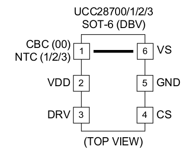
Pin Functions
| PIN | I/O | DESCRIPTION | ||
|---|---|---|---|---|
| NAME | UCC28700 | UCC28701/2/3 | ||
| NO. | NO. | |||
| CBC | 1 | — | I | Cable Compensation (CBC) is a programming pin for compensation of cable voltage drop. Cable compensation is programmed with a resistor to GND. |
| CS | 4 | 4 | I | Current Sense (CS) input connects to a ground-referenced current-sense resistor in series with the power switch. The resulting voltage is used to monitor and control the peak primary current. A series resistor can be added to this pin to compensate the peak switch current levels as the AC-mains input varies. |
| DRV | 3 | 3 | O | Drive (DRV) is an output used to drive the gate of an external high voltage MOSFET switching transistor. |
| GND | 5 | 5 | — | The Ground (GND) pin is both the reference pin for the controller and the low-side return for the drive output. Special care should be taken to return all AC decoupling capacitors as close as possible to this pin and avoid any common trace length with analog signal return paths. |
| NTC | — | 1 | I | NTC is an interface to an external NTC (negative temperature coefficient) resistor for remote temperature sensing. Pulling this pin low shuts down PWM action. |
| VDD | 2 | 2 | — | VDD is the bias supply input pin to the controller. A carefully-placed bypass capacitor to GND is required on this pin. |
| VS | 6 | 6 | I | Voltage Sense (VS) is an input used to provide voltage and timing feedback to the controller. This pin is connected to a voltage divider between an auxiliary winding and GND. The value of the upper resistor of this divider is used to program the AC-mains run and stop thresholds and line compensation at the CS pin. |