SLUSC36B November   2015  – January 2016 UCC28881

PRODUCTION DATA.  

  1. Features
  2. Applications
  3. Description
  4. Revision History
  5. Device Comparison
  6. Pin Configuration and Functions
  7. Specifications
    1. 7.1 Absolute Maximum Ratings
    2. 7.2 ESD Ratings
    3. 7.3 Recommended Operating Conditions
    4. 7.4 Thermal Information
    5. 7.5 Electrical Characteristics
    6. 7.6 Switching Characteristics
    7. 7.7 Typical Characteristics
  8. Detailed Description
    1. 8.1 Overview
    2. 8.2 Functional Block Diagram
    3. 8.3 Feature Description
    4. 8.4 Device Functional Modes
      1. 8.4.1 Start-Up Operation
      2. 8.4.2 Feedback and Voltage Control Loop
      3. 8.4.3 PWM Controller
      4. 8.4.4 Current Limit
      5. 8.4.5 Inductor Current Runaway Protection
      6. 8.4.6 Over Temperature Protection
  9. Application and Implementation
    1. 9.1 Application Information
    2. 9.2 Typical Application
      1. 9.2.1 13-V, 225-mA High-Side Buck Converter
        1. 9.2.1.1 Design Requirements
        2. 9.2.1.2 Detailed Design Procedure
          1. 9.2.1.2.1 Input Stage (RF, D2, D3, C1, C2, L2)
          2. 9.2.1.2.2 Regulator Capacitor (CVDD)
          3. 9.2.1.2.3 Freewheeling Diode (D1)
          4. 9.2.1.2.4 Output Capacitor (CL)
          5. 9.2.1.2.5 Pre-Load Resistor (RL)
          6. 9.2.1.2.6 Inductor (L1)
          7. 9.2.1.2.7 Feedback Path (CFB, RFB1 and RFB2) and Load Resistor (RL)
        3. 9.2.1.3 Application Curves
      2. 9.2.2 Additional UCC28881 Application Topologies
        1. 9.2.2.1 Low-Side Buck and LED Driver - Direct Feedback (Level Shifted)
        2. 9.2.2.2 High-Side Buck Converter
        3. 9.2.2.3 Non-Isolated, Low-Side Buck-Boost Converter
        4. 9.2.2.4 Non-Isolated, High-Side Buck-Boost Converter
        5. 9.2.2.5 Non-Isolated Flyback Converter
        6. 9.2.2.6 Isolated Flyback Converter
  10. 10Power Supply Recommendations
  11. 11Layout
    1. 11.1 Layout Guidelines
    2. 11.2 Layout Example
  12. 12Device and Documentation Support
    1. 12.1 Device Support
      1. 12.1.1 Third-Party Products Disclaimer
    2. 12.2 Community Resources
    3. 12.3 Trademarks
    4. 12.4 Electrostatic Discharge Caution
    5. 12.5 Glossary
  13. 13Mechanical, Packaging, and Orderable Information

Package Options

Mechanical Data (Package|Pins)
Thermal pad, mechanical data (Package|Pins)
Orderable Information

6 Pin Configuration and Functions

D package
8-Pin SOIC
Top View
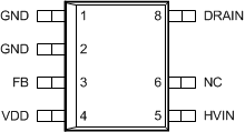
UCC28881 pin_lusc36.gif

Pin Functions

PIN I/O DESCRIPTION
NAME NO.
DRAIN 8 P Drain pin
FB 3 I Feedback terminal
GND 1 G Ground
GND 2 G Ground
HVIN 5 P Supply pin
NC 6 N/C Not internally connected
VDD 4 O Supply pin, supply is provided by internal LDO