SLUS769D July 2013 – December 2016 UCC28910 , UCC28911
PRODUCTION DATA.
- 1 Features
- 2 Applications
- 3 Description
- 4 Simplified Schematic
- 5 Revision History
- 6 Device Comparison Table
- 7 Pin Configuration and Functions
- 8 Detailed Pin Description
- 9 Specifications
-
10Detailed Description
- 10.1 Overview
- 10.2 Functional Block Diagram
- 10.3 Feature Description
- 10.4 Device Functional Modes
-
11Applications and Implementation
- 11.1 Application Information
- 11.2
Typical Application
- 11.2.1
Battery Charger, 5 V, 6 W
- 11.2.1.1 Design Requirements
- 11.2.1.2
Detailed Design Procedure
- 11.2.1.2.1 Power Handling Curves
- 11.2.1.2.2 Input Stage Design and Bulk Capacitance
- 11.2.1.2.3 Transformer Turns Ratio
- 11.2.1.2.4 Output Capacitance
- 11.2.1.2.5 VDD Capacitance, CVDD
- 11.2.1.2.6 VS Resistor Divider
- 11.2.1.2.7 RVDD Resistor and Turn Ratio
- 11.2.1.2.8 Transformer Input Power
- 11.2.1.2.9 RIPK Value
- 11.2.1.2.10 Transformer Primary Inductance Value
- 11.2.1.2.11 Pre-Load
- 11.2.1.2.12 DRAIN Voltage Clamp Circuit
- 11.2.2 Application Curves
- 11.2.3 Multi-Output Converter with UCC2891x Devices
- 11.2.4 Do’s and Don'ts
- 11.2.1
Battery Charger, 5 V, 6 W
- 12Power Supply Recommendations
- 13Layout
- 14Device and Documentation Support
- 15Mechanical, Packaging, and Orderable Information
Package Options
Mechanical Data (Package|Pins)
- D|7
Thermal pad, mechanical data (Package|Pins)
Orderable Information
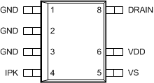
7 Pin Configuration and Functions
D (SOIC) Package
7 Pins
(Top View)

Pin Functions
| PIN | I/O(1) | DESCRIPTION | |
|---|---|---|---|
| NAME | NO. | ||
| DRAIN | 8 | P | DRAIN, the drain of the internal power FET, but also the input for the high-voltage current source used to start up the device. |
| GND | 1 | G | The ground pins (GND) are both the reference pins for the controller and the low-side return for the drive output. Special care should be taken to return all AC decoupling as close as possible to this pin and avoid any common trace length with analog signal return paths. |
| 2 | |||
| 3 | |||
| IPK | 4 | O | IPK is used to set the maximum peak current flowing in the power FET that is proportional to the maximum output current. |
| N/A | 7 | N/A | This pin is not present to provide enough distance between high voltage pin (DRAIN) and VDD pins. |
| VDD | 6 | P | VDD is the supply pin to the controller. A carefully placed bypass capacitor to GND is required on this pin. |
| VS | 5 | I | Voltage Sense (VS) is used to provide voltage and timing feedback to the controller. Normally this pin is connected to a voltage divider between an auxiliary winding and ground. The value of the upper resistor of this divider is used to program low line thresholds. |
(1) P = Supply, G = Ground, I = Input, O = output