SLVSAC8D November 2010 – April 2019 UCD90160
PRODUCTION DATA.
- 1 Features
- 2 Applications
- 3 Description
- 4 Revision History
- 5 Pin Configuration and Functions
- 6 Specifications
-
7 Detailed Description
- 7.1 Overview
- 7.2 Functional Block Diagram
- 7.3 Feature Description
- 7.4
Device Functional Modes
- 7.4.1 Power-Supply Sequencing
- 7.4.2 Pin-Selected Rail States
- 7.4.3 Voltage Monitoring
- 7.4.4 Fault Responses and Alert Processing
- 7.4.5 Shut Down All Rails and Sequence On (Resequence)
- 7.4.6 GPIOs
- 7.4.7 GPO Control
- 7.4.8 GPO Dependencies
- 7.4.9 GPI Special Functions
- 7.4.10 Power-Supply Enables
- 7.4.11 Cascading Multiple Devices
- 7.4.12 PWM Outputs
- 7.4.13 Programmable Multiphase PWMs
- 7.4.14 Margining
- 7.4.15 System Reset Signal
- 7.4.16 Watch Dog Timer
- 7.4.17 Run Time Clock
- 7.4.18 Data and Error Logging to Flash Memory
- 7.4.19 Brownout Function
- 7.4.20 PMBus Address Selection
- 7.5 Programming
- 8 Application and Implementation
- 9 Power Supply Recommendations
- 10Layout
- 11Device and Documentation Support
- 12Mechanical, Packaging, and Orderable Information
Package Options
Mechanical Data (Package|Pins)
- RGC|64
Thermal pad, mechanical data (Package|Pins)
- RGC|64
Orderable Information
3 Description
The UCD90160 is a 16-rail PMBus/I2C addressable power-supply sequencer and monitor. The device integrates a 12-bit ADC for monitoring up to 16 power-supply voltage inputs. Twenty-six GPIO pins can be used for power supply enables, power-on reset signals, external interrupts, cascading, or other system functions. Twelve of these pins offer PWM functionality. Using these pins, the UCD90160 offers support for margining, and general-purpose PWM functions.
Specific power states can be achieved using the Pin-Selected Rail States feature. This feature allows with the use of up to 3 GPIs to enable and disable any rail. This is useful for implementing system low-power modes and the Advanced Configuration and Power Interface (ACPI) specification that is used for hardware devices.
The TI Fusion Digital Power™ designer software is provided for device configuration. This PC-based graphical user interface (GUI) offers an intuitive interface for configuring, storing, and monitoring all system operating parameters.
Device Information(1)
| PART NUMBER | PACKAGE | BODY SIZE (NOM) |
|---|---|---|
| UCD90160 | VQFN (64) | 9.00 mm × 9.00 mm |
- For all available packages, see the orderable addendum at the end of the data sheet.
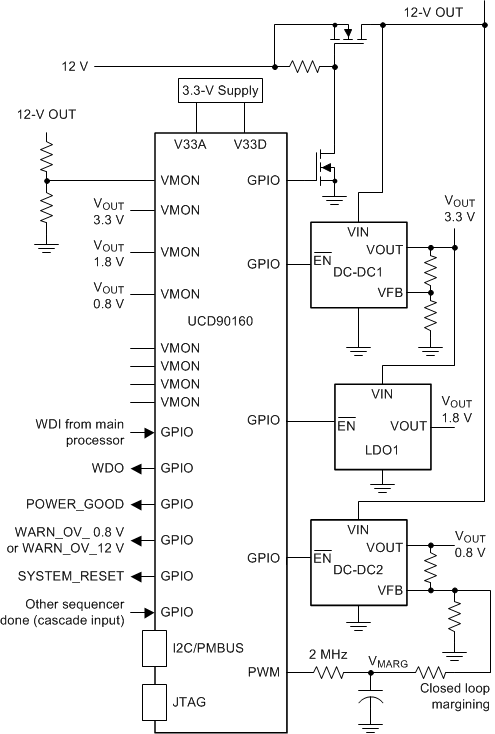
Simplified Application Schematic
